Semiconductor structure

A technology of semiconductors and ball pads, applied in semiconductor devices, semiconductor/solid-state device parts, electric solid-state devices, etc.

Pending Publication Date: 2022-07-29
MEDIATEK INC
View PDF0 Cites 0 Cited by
  • Summary
  • Abstract
  • Description
  • Claims
  • Application Information

AI Technical Summary

Problems solved by technology

Impedance matching presents challenges for radio frequency (RF) and microwave circuit design because the window of error decreases with increasing frequency

Method used


Image

  • Semiconductor structure
  • Semiconductor structure
  • Semiconductor structure

Examples


Embodiment Construction

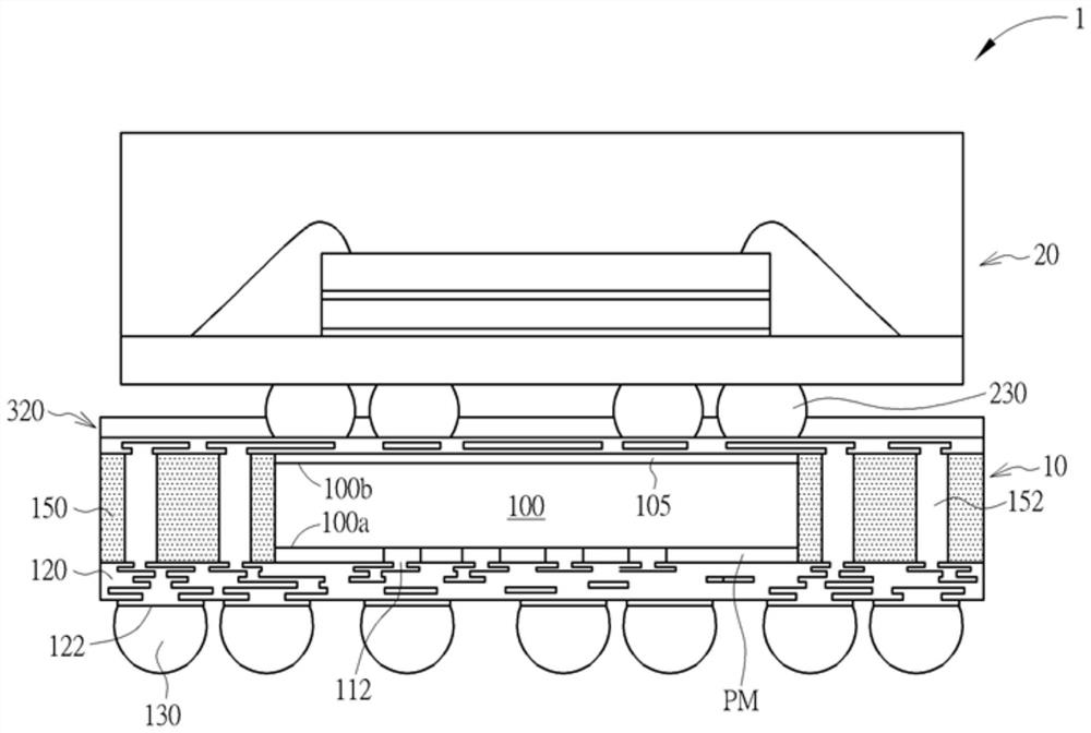
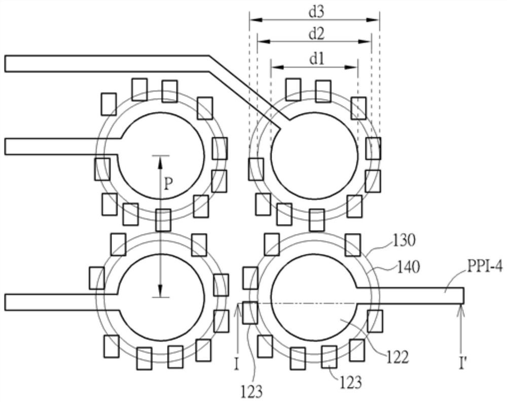
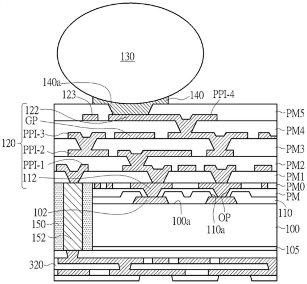
[0044] The following description is a preferred embodiment of the present invention, which is only used to illustrate the technical characteristics of the present invention, but not to limit the scope of the present invention. Certain terms are used throughout the specification and claims to refer to particular elements, it being understood by those skilled in the art that manufacturers may refer to the same elements by different names. Therefore, the present specification and claims do not take the difference in name as a way to distinguish elements, but take the difference in function of the elements as a basis for distinction. The terms "element," "system," and "apparatus" as used in the present invention can be a computer-related entity, wherein the computer can be hardware, software, or a combination of hardware and software. The terms "comprising" and "including" mentioned in the following description and claims are open-ended terms and should be interpreted as meaning "...


PUM

PropertyMeasurementUnit
diameteraaaaaaaaaa
diameteraaaaaaaaaa
thicknessaaaaaaaaaa

Abstract

The invention provides a semiconductor structure capable of improving impedance control. A semiconductor structure includes a semiconductor die having an active surface, a passivation layer covering the active surface of the semiconductor die, and a post-passivation interconnect (PPI) layer disposed over the passivation layer. The PPI layer includes a ball pad having a first diameter. The polymer layer covers the periphery of the ball pad. An under bump metal (UBM) layer is disposed on the ball pad. The second diameter of the UBM layer is greater than the first diameter of the ball pad. A solder ball is mounted on the UBM layer.

Description

technical field [0001] Embodiments of the present invention relate generally to the field of semiconductor packaging, and more particularly, the present invention relates to semiconductor packaging with novel ball pad designs for semiconductor packaging, particularly RDL-based packaging. Background technique [0002] Advances in the semiconductor field have raised a number of issues and challenges in signal integrity (SI) and power integrity (PI). Package interconnects are discontinuities in signal and power transmission and are susceptible to a variety of factors including crosstalk, parasitic coupling, impedance mismatch, simultaneous switching noise (SSN) and electromagnetic interference (EMI). [0003] Impedance control is an important issue in high-speed circuit and system design. Impedance matching presents challenges for radio frequency (RF) and microwave circuit design because the error window decreases with increasing frequency. High-speed digital circuits require...

Claims


Application Information

Patent Timeline
Patent Type & Authority Applications(China)
IPC IPC(8): H01L23/498
CPCH01L23/49816H01L23/49838H01L24/20H01L2224/73267H01L2224/32225H01L2224/04105H01L2224/12105H01L25/105H01L25/0657H01L2224/32145H01L2224/48227H01L2224/73265H01L2924/15311H01L2225/1035H01L2225/1041H01L2225/1058H01L2224/0401H01L2224/05572H01L2224/05569H01L2224/05008H01L2224/05583H01L2224/11849H01L2224/11462H01L2224/11334H01L2224/1132H01L2224/13147H01L2224/13139H01L2224/13111H01L2224/02235H01L2224/02255H01L2924/3512H01L2224/05666H01L2224/05684H01L2224/05655H01L2224/05644H01L2224/05647H01L2224/05671H01L2924/3011H01L2924/3025H01L24/05H01L24/11H01L24/13H01L24/48H01L24/32H01L24/73H01L24/19H01L2224/05012H01L2224/05555H01L2224/05559H01L23/3171H01L23/3128H01L23/5389H01L2224/48225H01L2924/00012H01L2924/00014H01L2924/00H01L23/49822
Inventor 颜江霖郭哲宏
Owner MEDIATEK INC
Why Eureka
Try Eureka