High-density BGA printed circuit board wiring method

A technology for printed circuit boards and spherical contacts, which is used in printed circuits, printed circuit manufacturing, electrical components, etc. It can solve problems such as thin board thickness and difficulty in passing two vias through signal lines, and achieve easy-to-guaranteed yields. Conducive to impedance control and easy-to-achieve effects

Inactive Publication Date: 2008-12-03
HUAWEI TECH CO LTD
View PDF4 Cites 0 Cited by
  • Summary
  • Abstract
  • Description
  • Claims
  • Application Information

AI Technical Summary

Problems solved by technology

[0013] The technical problem to be solved by the present invention is to overcome the shortcomings of the prior art that the board thickness is thin due to the small via holes of the small-pitch BGA, and the difficulty of crossing the signal line between the two via holes, and provide a method for PCB routing of high-density BGA , so that the diameter of the via hole can be increased, the thickness of the board can be increased, and the signal line can pass through the two via holes

Method used


Image

  • High-density BGA printed circuit board wiring method
  • High-density BGA printed circuit board wiring method
  • High-density BGA printed circuit board wiring method

Examples


Embodiment Construction

[0027] Below according to accompanying drawing and embodiment the present invention will be described in further detail:

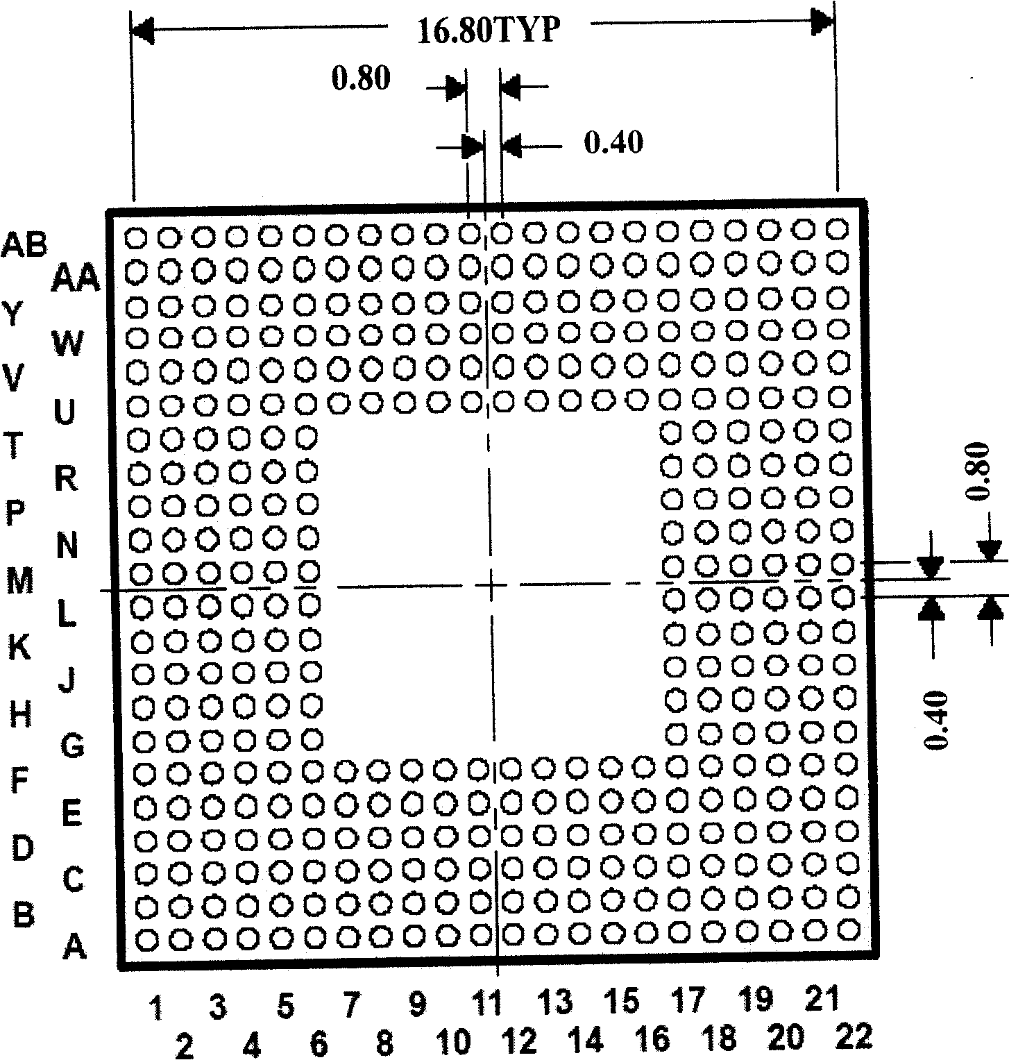
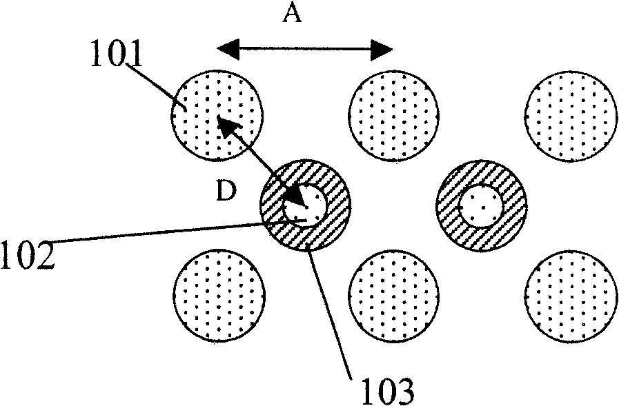
[0028] For small-pitch ball contact array printed circuit boards (that is, ball contact array printed circuit boards with a center-to-center spacing of 0.8 mm or less between adjacent ball contacts), the present invention provides a wiring method First, according to the size parameters and process requirement parameters of the small-pitch BGA pads of the printed circuit board, the maximum diameter d2 of the via top-layer pad is calculated, that is, the aforementioned distance between the device pad and the center of the via pad ( Assumed to be D), and the diameter of the device pad (assumed to be d1), the minimum spacing allowed from the device pad to the via pad (assumed to be D2) for calculation, and the calculation of the maximum diameter (d2) of the via top layer pad The formula is: d2=(D-D2-d1 / 2)*2. According to the maximum diameter of the pad on the...


PUM


Abstract

The method for high-dense ball contact matrix PEB routing comprises: for said PCB with small span, according to size parameters and technical requirements of BGA bonding pad, calculating maximal diameter of past-hole top bonding pad to obtain a hole-past hole diameter larger a little than said maximal diameter for PCB; if two adjacent past-holes do not conduct electricity on the signal layer, then gets rid of said past-hole pad or decreases diameter of said common pad to cross a signal wire between two holes. This invention can increase past-hole diameter and plate thickness benefit to control impedance and solve problem hard to cross signal wire.

Description

technical field [0001] The invention relates to the technical field of circuit design, in particular to a method for wiring a printed circuit board with a high-density spherical contact array. Background technique [0002] With the rapid development of science and technology, the integration and complexity of chips are getting higher and higher, and the design and manufacturing of PCB (printed circuit board) are becoming more and more difficult. PCB design must consider the possible problems that may be encountered during PCB production and processing. For various problems, the quality of the PCB depends on the design. Only by fully considering the processing technology limit of the PCB manufacturer during the design process can it be possible to ensure the yield rate of the PCB during production. The following table 1 is some setting parameters recommended by domestic mainstream PCB manufacturers. If the recommended value is exceeded, PCB will form a process bottleneck in m...

Claims


Application Information

Patent Timeline
Patent Type & Authority Patents(China)
IPC IPC(8): H05K3/40H05K3/00
Inventor 刘卫东贾荣华唐艳梅
Owner HUAWEI TECH CO LTD
Why Eureka
Try Eureka