Pixel defining layer and manufacturing method thereof

A technique for defining a pixel definition layer and a manufacturing method, which is applied in semiconductor/solid-state device manufacturing, electrical components, electrical solid-state devices, etc., and can solve the problems of complicated plasma processing steps, high purity requirements, and inability to obtain liquid repellency, etc. Achieve the effect of material saving, high material utilization rate and low manufacturing cost

Active Publication Date: 2017-10-13
TCL CHINA STAR OPTOELECTRONICS TECH CO LTD
View PDF10 Cites 25 Cited by
  • Summary
  • Abstract
  • Description
  • Claims
  • Application Information

AI Technical Summary

Problems solved by technology

The general pixel definition layer in the prior art does not meet this requirement
[0006] In some existing technologies, an inorganic layer is prepared on the side of the dam body to achieve lyophilicity. In addition, the dam body needs to be treated with plasma infusion. The preparation process of this structure is very complicated. Prepare an inorganic material layer on top of the dam body, and then remove the inorganic layer on the upper surface of the dam body, leaving an inorganic layer covering the side of the dam body, but this can only achieve the lyophilicity of the side of the dam body, while the upper surface of the dam body cannot obtain lyophobicity , failed to meet the above-mentioned lyophobic requirement that ink droplets can easily flow into the pixel sub-region, so this prior art also needs to perform plasma hydrophobic treatment on the dam body, so that the upper surface of the dam body becomes hydrophobic Liquidity, the plasma treatment process needs more time, and has higher requirements on the vacuum degree and purity of the processing chamber, and the whole plasma treatment steps are relatively complicated, and the whole preparation method of the pixel defining layer in the prior art includes spraying Ink preparation and plasma hydrophobic treatment, the preparation process is complicated, the cost is high, and the required process fixtures are various, which is not ideal

Method used


Image

  • Pixel defining layer and manufacturing method thereof
  • Pixel defining layer and manufacturing method thereof
  • Pixel defining layer and manufacturing method thereof

Examples


Embodiment 1

[0051] see Figure 7 , the present invention provides a first embodiment of a method for manufacturing a pixel defining layer, which includes:

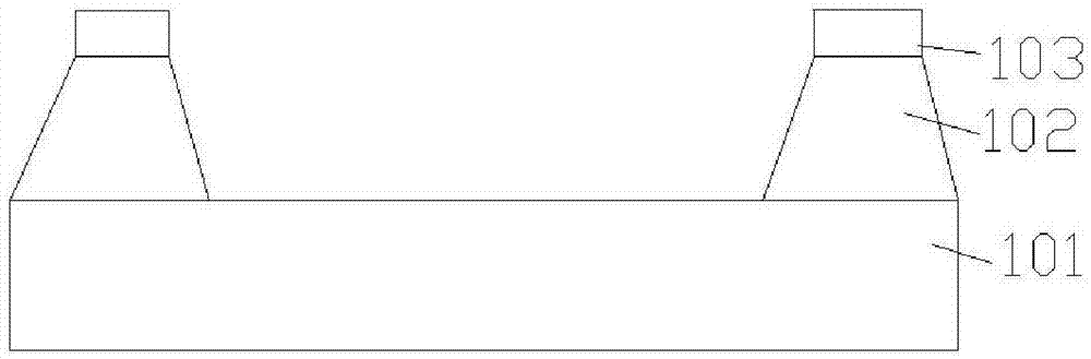
[0052] Prepare the first defined layer on the substrate 101, wherein the first defined layer includes a dam body 102 partially covered on the substrate 101, generally, the material of the dam body 102 is a common defined layer material, which does not require liquid-repellent properties, and more Further, a black light-shielding material can be arranged under the dam body 102, or the dam body 102 is made of black light-shielding material to prevent lateral light leakage;

[0053] Prepare a layer of lyophobic film 103 on the substrate 101 and the first defining layer;

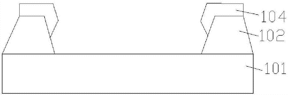
[0054] A photoresist layer 113 is prepared on the top of the dam 102 located in the first defining layer. Specifically, a layer of photoresisting layer 113 can be prepared on the entire substrate 101 and the first defining layer, and then through the yellow light proce...


PUM


Abstract

According to the invention, a first defining layer of a pixel defining layer comprises dam bodies locally covering a substrate; second defining layers are arranged at the tops of the dam bodies; and the second defining layers are made of a lyophobic material. A manufacturing method of the pixel defining layer disclosed by the invention comprises the steps of: preparing the first defining layer on the substrate; preparing one layer of lyophobic material on the substrate and the first defining layer; and by the etching process, removing the lyophobic material between the dam bodies to obtain the second defining layers covering the dam bodies of the first defining layer. According to the pixel defining layer disclosed by the invention, hydrophobic layers are arranged at the tops of the dam bodies, and a material of the substrate has the lyophilic property, so that the requirements for top lyophobicity and bottom lyophilic property of the pixel defining layer are met; and the manufacturing method of the pixel defining layer disclosed by the invention is simple, low in manufacturing cost and very simple and convenient in process flow.

Description

technical field [0001] The invention relates to the field of display technology, in particular to a pixel defining layer and a manufacturing method thereof. Background technique [0002] Due to the advantages of self-illumination, no need for backlight, high contrast, thin thickness, wide viewing angle, fast response speed, and flexible panels, OLED displays are considered to be the next-generation flat-panel display emerging application technology. [0003] OLEDs have an anode, an organic functional layer, and a cathode formed on the substrate in sequence. At present, most OLED functional material layers and cathode metal layer films are prepared by vacuum thermal evaporation, that is, organic small molecule materials are heated in a vacuum chamber to make It is sublimated or melted and gasified into material vapor, which is deposited on the glass substrate through the openings of the metal mask. However, the high cost of vacuum thermal evaporation limits the wide-scale com...

Claims


Application Information

Patent Timeline
Patent Type & Authority Applications(China)
IPC IPC(8): H01L27/32H01L51/56
CPCH10K59/122H10K71/135H10K71/00
Inventor 陈黎暄陈孝贤
Owner TCL CHINA STAR OPTOELECTRONICS TECH CO LTD
Why Eureka
Try Eureka