LED epitaxial structure and preparation method thereof

An epitaxial structure, non-doping technology, applied in the direction of electrical components, circuits, semiconductor devices, etc., can solve the problems of unstable structure, many impurities, complex process, etc., achieve small size, large light-emitting area, and reduce dislocation density Effect

Active Publication Date: 2017-10-13
TAIYUAN UNIV OF TECH
View PDF4 Cites 3 Cited by
  • Summary
  • Abstract
  • Description
  • Claims
  • Application Information

AI Technical Summary

Problems solved by technology

[0006] What the present invention aims to solve are the shortcomings of existing LED epitaxial structure preparation methods, such as many impurities, unstable structure, complicated process, etc., and provide an LED epitaxial structure with simple process and its preparation method

Method used


Image

  • LED epitaxial structure and preparation method thereof
  • LED epitaxial structure and preparation method thereof

Examples


Embodiment

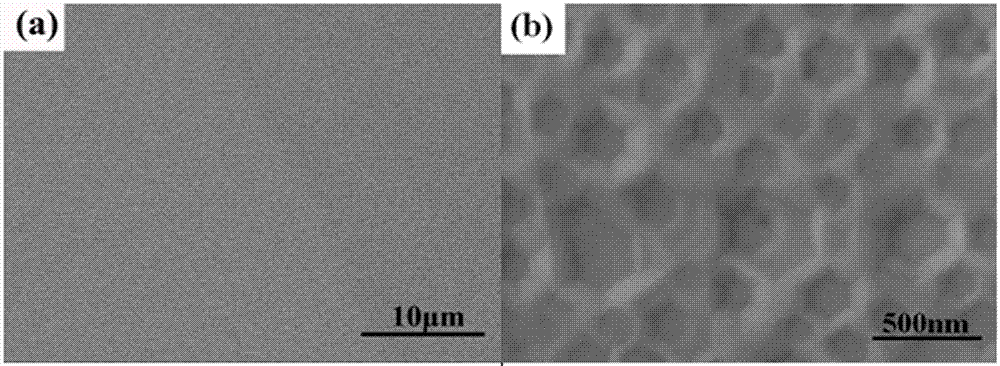
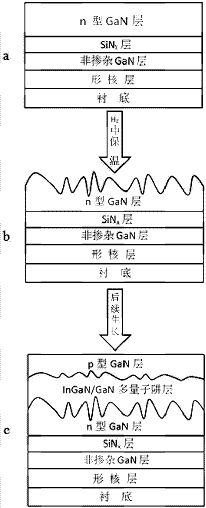
[0036] This embodiment provides a method for preparing an LED epitaxial structure, such as figure 2 As shown, the structure includes a sapphire substrate, a nucleation layer formed on the (111) crystal plane of the substrate, a non-doped GaN layer, a SiN x layer, n-type GaN layer, InGaN / GaN multiple quantum well layer, p-type GaN layer.

[0037] As an embodiment of the present invention, the thickness of the non-doped GaN layer in this embodiment is 1 μm; SiN x The thickness of the layer is 10nm; the thickness of the n-type GaN layer is 3μm; the InGaN / GaN multi-quantum well layer has three well barrier periods; the thickness of the p-type GaN layer is 3μm; the decomposition temperature is 1000°C; the decomposition time is 20min. As an alternative embodiment of the present invention, the thickness of the non-doped GaN layer is 100nm~1μm, SiN x The thickness of the layer is 10nm~100nm, the thickness of the n-type GaN layer is 1μm~3μm, the InGaN / GaN multi-quantum well layer is...


PUM

PropertyMeasurementUnit
thicknessaaaaaaaaaa
temperatureaaaaaaaaaa
thicknessaaaaaaaaaa

Abstract

The invention relates to an LED epitaxial structure and a preparation method thereof. The LED epitaxial structure comprises a sapphire substrate, and a nucleation layer, a non doped GaN layer, a SiNx layer, an n type GaN layer, an InGaN / GaN multiple quantum well layer and a p type GaN layer, which are stacked sequentially and formed on the crystal surface of the substrate (111); a high temperature insulation step in the H2 atmosphere is performed between the n type GaN layer and the InGaN / GaN multiple quantum well layer. The LED epitaxial structure preparation method utilizes the properties of GaN decomposition at a high temperature. In the process of high temperature decomposition of the n type GaN layer, the decomposition at the dislocations and other defects is occurred preferentially because the thermal stability is poor, and the H2 atmosphere helps to speed up decomposition, so that an irregular hill-shaped structure is formed; and after further growth steps, the LED epitaxial structure with many advantages is prepared.

Description

technical field [0001] The invention relates to the technical field of semiconductors, in particular to an LED epitaxial structure and a preparation method thereof. Background technique [0002] As the third-generation light source, LED has many advantages such as high brightness, low cost, long life, small size, energy saving and environmental protection. In recent years, with the maturity of technology and the reduction of cost, the LED market has ushered in explosive growth, and is gradually moving towards ordinary households, and is widely used in various fields such as lighting, display, and decoration. [0003] Since the advent of commercial GaN-based LEDs in 1996, it has gone through more than 20 years of development and has already become a mainstream product in the LED lighting market. However, there are still many problems to be solved in the preparation of GaN-based semiconductor materials. For example, the influence mechanism of growth process parameters on the ...

Claims


Application Information

Patent Timeline
Patent Type & Authority Applications(China)
IPC IPC(8): H01L33/00H01L33/02H01L33/22
CPCH01L33/007H01L33/02H01L33/22
Inventor 贾伟樊腾仝广运李天保翟光美许并社
Owner TAIYUAN UNIV OF TECH
Why Eureka
Try Eureka