

Preparation method of detection sample and detection method
A technology for testing samples and connectors, which is applied in the field of testing sample preparation, can solve problems such as insufficiently clear images and difficult detection, and achieve the effect of increasing clarity and reducing the difficulty of detection
Active Publication Date: 2017-10-20
SEMICON MFG INT (SHANGHAI) CORP +1
View PDF4 Cites 1 Cited by
- Summary
- Abstract
- Description
- Claims
- Application Information
AI Technical Summary
Problems solved by technology
However, the change of dielectric layer material and the narrowing of metal interconnect line width have brought great challenges to the detection and analysis of semiconductor devices
[0005] The image of the test sample prepared by the prior art is not clear enough under the microscope, making it difficult to detect
Method used
View moreImage
Smart ImageViewing Examples

Examples
preparation example Construction
[0033] Combining with a method for preparing a test sample, the reasons for the difficulty in the detection of the formed test sample are analyzed:
Login to View More PUM
| Property | Measurement | Unit |
|---|---|---|
| thickness | aaaaa | aaaaa |
Abstract
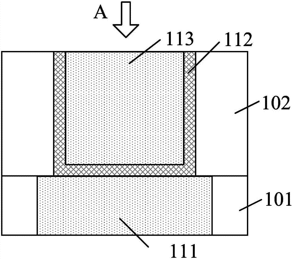
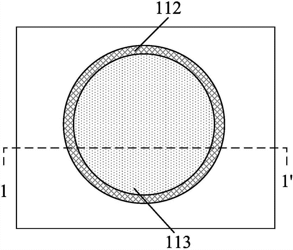
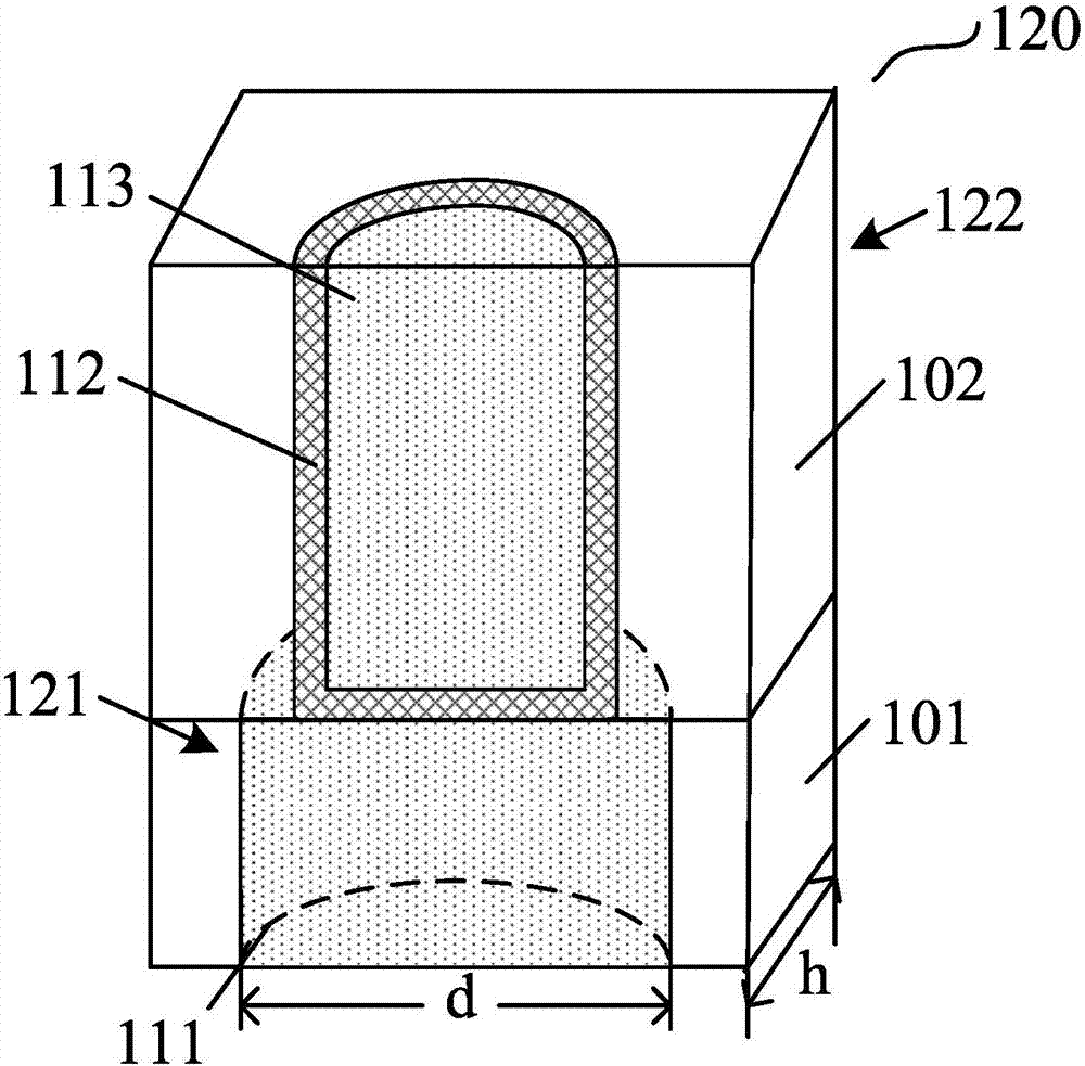
The invention provides a preparation method of a detection sample. The preparation method comprises the following steps: providing a semiconductor structure, wherein the semiconductor structure comprises a first connecting piece and a barrier layer located on the surface of the first connecting piece, the diffusion coefficient of the barrier layer is smaller than that of the first connecting piece, and atomic density difference between a dielectric layer and the barrier layer is larger than that between the first connecting piece and the barrier layer; performing section faultage treatment on the semiconductor structure to form a section film; performing diffusion treatment on the section film. By means of the diffusion treatment on the section film, the first connecting piece with larger diffusion coefficient is diffused into the dielectric layer. Besides, the atomic density difference between the dielectric layer located on a second side of the section film and the barrier layer is larger than that between the first connecting piece and the barrier layer. Therefore, after an image is formed by the detection sample, the definition of an image formed on the side wall of the barrier layer can be improved, and detection difficulty can be reduced.
Description
technical field [0001] The invention relates to the technical field of semiconductor manufacturing, in particular to a preparation method and a detection method of a detection sample. Background technique [0002] With the continuous advancement of semiconductor technology, the feature size of semiconductor devices is gradually reduced. The reduction of the feature size of semiconductor devices puts forward higher requirements on semiconductor technology. [0003] In semiconductor technology, the Damascene method is used in the manufacturing process of metal interconnect lines because it avoids the etching of metal copper. In order to ensure the yield rate of the damascene structure, it is necessary to detect and analyze the etching morphology and the deposition thickness of the barrier layer in the damascene structure through a transmission electron microscope (TEM). [0004] The reduction of critical dimensions of semiconductor devices makes semiconductor devices suffer ...
Claims
Login to View More Application Information
Patent Timeline
 Patent Type & AuthorityApplications(China)
IPC IPC(8): G01N1/28
CPCG01N1/28
Inventor胡敏达袁光杰何其暘陈柳段淑卿
OwnerSEMICON MFG INT (SHANGHAI) CORP