
3D-Printed Conductive Compositions Anticipating or Indicating Structural Damage
A 3D printing, composite technology, applied to conductive layers on insulating carriers, conductive coatings, equipment for manufacturing conductive/semi-conductive layers, etc., can solve problems such as low conductivity and achieve the effect of increasing conductivity
- Summary
- Abstract
- Description
- Claims
- Application Information
AI Technical Summary
Problems solved by technology
Method used
Image

Examples
example 1
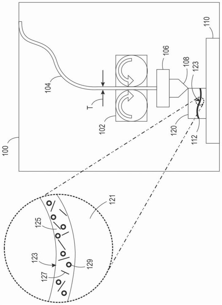
[0066] By extruding a polymer substrate (polycaprolactone; "PCL") with 10% by weight of multi-walled carbon nanotubes (MWNT) together with 30% by weight of silver (Ag) flakes on a Haake twin-screw extruder Conductive composite segments were prepared by melt mixing at 30 rpm for 30 minutes. The resulting material was cryogenically ground and the ground compound was extruded into filaments using a melt flow indexer (MFI) and a modified die. Extrusion conditions on the MFI included a 1.8 mm hole and a 16.96 kg weight in order to produce the final filament. The final filament has a diameter of about 1.75 mm.
example 2
[0068] A 10 cm cross-section of the extruded filament of Example 1 with the tip coated with silver paint was used to measure electrical resistance in order to calculate bulk conductivity. Resistance measurements are done using a digital multimeter. The bulk conductivity was calculated using Equation 1 above.
example 3
[0070] A composite similar to that of Example 1 was prepared, but using 30% by weight of Ag nanoparticles instead of Ag flakes.
PUM
| Property | Measurement | Unit |
|---|---|---|
| electrical conductivity | aaaaa | aaaaa |
| size | aaaaa | aaaaa |
| size | aaaaa | aaaaa |
Abstract
Description
Claims
Application Information