Organic-amidine-molecule n-type dopant and application thereof in semiconductor photoelectric devices

A dopant and organic amidine technology, which is applied to the n-type dopant of organic amidine molecules and its application in semiconductor optoelectronic devices, can solve the problems of high development cost, difficult solution preparation, poor effect, etc., and achieve improved device The effect of high performance, simple doping process, and wide application prospects

Active Publication Date: 2017-12-22
HUAZHONG UNIV OF SCI & TECH +1
View PDF3 Cites 7 Cited by
  • Summary
  • Abstract
  • Description
  • Claims
  • Application Information

AI Technical Summary

Problems solved by technology

[0005] Aiming at the above defects or improvement needs of the prior art, the present invention provides an organic amidine molecular n-type dopant and its application in semiconductor optoelectronic devices, thereby solving the problems of high development cost, difficulty in solution preparation and Poor technical issues

Method used


Image

  • Organic-amidine-molecule n-type dopant and application thereof in semiconductor photoelectric devices
  • Organic-amidine-molecule n-type dopant and application thereof in semiconductor photoelectric devices
  • Organic-amidine-molecule n-type dopant and application thereof in semiconductor photoelectric devices

Examples


Embodiment 1

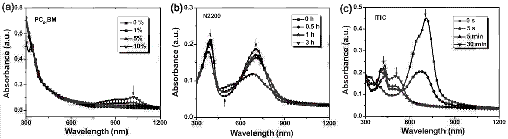
[0044] DBU to PC 61 BM, N2200 and ITIC for n-doping

[0045] According to different processes, use DBU to PC 61 BM, N2200 and ITIC are n-doped. First place the PC in a glove box filled with nitrogen 61 BM is dissolved in spectral pure chlorobenzene solvent, and the concentration of the resulting solution is 20 mg / ml. Then on the PC 61 Add DBU of different quality to the BM solution, heat and stir overnight at 50°C to achieve the 61 Doping of BM. The above-mentioned solutions with different doping concentrations were spin-coated into a film at a rotation speed of 1000 rpm, and the ultraviolet-visible absorption spectrum of the obtained film is as follows figure 1 (a). Preferably, the doping concentration for the electron transport layer of the perovskite battery device is 0.1 wt%. Take 50 microliters of the mixed solution with a doping concentration of 0.1 wt% and spin-coated on the surface of the prepared perovskite, which can be used as the battery electron transport layer. S...

Embodiment 2

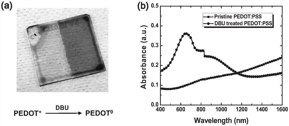
[0047] DBU reduction conductive polymer PEDOT: PSS

[0048] PEDOT:PSS (PH1000) was spin-coated on a glass substrate at a rotation speed of 1000 rpm, and then placed on a hot stage at 140°C and annealed for 10 minutes to obtain a light blue PEDOT:PSS film, as follows figure 2 (a) Shown. Cut the glass sheet in half and place half of it in a watch glass with DBU, and place the watch glass on a hot table at 100°C for 5 minutes. Observe that the color of the PEDOT:PSS film gradually darkens To dark blue, indicating that PEDOT: PSS was restored by DBU. figure 2 (b) is the ultraviolet-visible absorption spectrum of PEDOT: PSS before and after being processed by DBU. It is obvious that the absorption of PEDOT: PSS in the visible spectral region becomes stronger after being reduced.

Embodiment 3

[0050] PC 61 Change of conductivity before and after BM doping

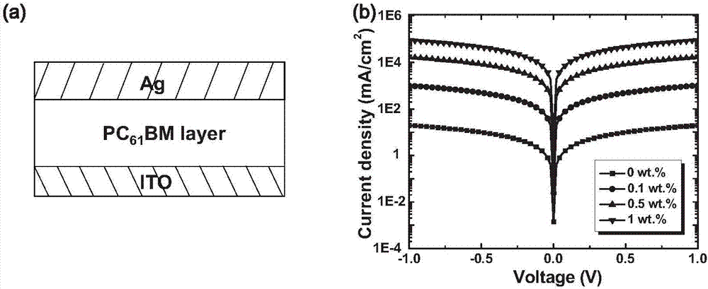
[0051] PC 61 The device structure of the conductivity test before and after BM doping is indium tin oxide glass / [6,6]-phenyl C 61 Methyl Butyrate / Silver (ITO / PC 61 BM layer / Ag). Among them, the bottom electrode is ITO conductive glass (indium tin oxide conductive glass), and the middle is PC before and after doping 61 BM layer, the top electrode is Ag, the structure is as image 3 (a). The specific preparation method of Example 3 is as follows:

[0052] (1) ITO glass is washed with soapy water, deionized water, acetone, isopropanol, and then ultrasonically cleaned by Plasma.

[0053] (2) In a glove box filled with nitrogen atmosphere, take the PC configured in Example 1 above 61 The BM solution was spin-coated on the cleaned ITO glass at a speed of 2000 rpm to obtain a 40nm thick pure PC 61 BM or doped PC 61 BM film. Then, a layer of 70nm Ag was evaporated by a vacuum coating apparatus.

[0054] (3) Test the current-vo...


PUM


Abstract

The invention discloses an organic-amidine-molecule n-type dopant and an application thereof in semiconductor photoelectric devices. The n-type dopant is of an organic amidine molecule and is mixed with a receptor material, or the receptor material is directly exposed in a steam atmosphere of the n-type dopant, and thus, the n doping of the receptor material is achieved. According to the organic-amidine-molecule n-type dopant and the application thereof in the semiconductor photoelectric devices, by adding the n-type dopant into an organic n-type semiconductor, properties such as electric conductivity, work function and electron mobility of the organic semiconductor can be regulated; and after the receptor material is subjected to n doping by the n-type dopant, the receptor material is applied to perovskite solar cells, organic solar cells, organic light emitting diodes and organic field effect transistors.

Description

Technical field [0001] The invention belongs to the field of semiconductor devices, and more specifically, relates to an organic amidine molecule n-type dopant and its application in semiconductor optoelectronic devices. Background technique [0002] Organic semiconductors are a new class of materials that have been widely used in semiconductor photovoltaic devices such as organic light-emitting diodes, organic field effect transistors, organic solar cells, and perovskite solar cells. In these devices, charge injection and extraction are often involved, especially between the organic semiconductor and the electrode. Therefore, the efficiency of charge transfer will greatly affect the performance of the device. The conductivity of the organic semiconductor material itself and the degree of matching between the Fermi level of the material and the work function of the adjacent electrode are crucial factors that affect the charge transfer. [0003] Effective doping of organic semicon...

Claims


Application Information

Patent Timeline
Patent Type & Authority Applications(China)
IPC IPC(8): C07D487/04C07D233/56C07C259/14C07C257/12C07C257/14C07C257/18H01L51/30H01L51/46H01L51/54
CPCC07C257/12C07C257/14C07C257/18C07C259/14C07D233/56C07D487/04H10K85/60H10K85/654H10K85/6572Y02E10/549
Inventor 周印华胡林蒋友宇刘铁峰覃飞熊思醒
Owner HUAZHONG UNIV OF SCI & TECH
Why Eureka
Try Eureka