Three-dimensional stack structure of thin-film ceramic circuit

A three-dimensional stacking and thin-film technology, which is applied in the direction of circuits, electrical components, and electrical solid devices, can solve the problems of large restrictions, large product volume, and high cost, and achieve the goal of improving product adaptability, production efficiency, and integration. Effect

Active Publication Date: 2017-10-20
SOUTHWEST CHINA RES INST OF ELECTRONICS EQUIP
View PDF4 Cites 7 Cited by
  • Summary
  • Abstract
  • Description
  • Claims
  • Application Information

AI Technical Summary

Problems solved by technology

Its shortcomings mainly lie in: on the one hand, all functional units are tiled and installed in the two-dimensional direction of the substrate, the interconnection design of embedded devices is relatively complicated, the product is large in size, high in cost, and it is not convenient for independent testing; on the other hand, LTCC Or the PCB substrate process has great limitations in terms of graphic line width / line spacing, arbitrary layer interconnection, passive device integration, etc., and it cannot integrate some high-performance units

Method used


Image

  • Three-dimensional stack structure of thin-film ceramic circuit
  • Three-dimensional stack structure of thin-film ceramic circuit
  • Three-dimensional stack structure of thin-film ceramic circuit

Examples


specific Embodiment 1

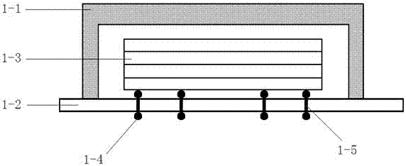
[0018] A three-dimensional stacked structure of thin-film ceramic circuits, between two adjacent layers of thin-film ceramic substrates, through ball planting welding or prefabricated pad 3-1 welding, so as to realize the stacking of more than three layers of thin-film ceramic circuit substrates; using solid metal through holes Realize conductive connection of any layer; include partial electromagnetic self-shielding structure of chips 2-4 and / or passive components; said partial electromagnetic self-shielding structure includes upper and lower metal layers and side solid metal through holes.

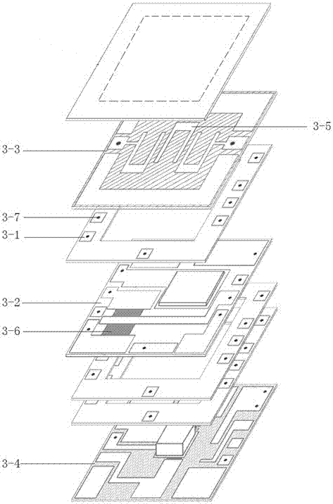
[0019] The two adjacent layers are soldered by ball bonding or prefabricated pads, and the image 3 In the specific embodiment shown, the stacking of substrates is realized by welding prefabricated pads between two adjacent layers. Similarly, ball planting (such as BGA ball planting) can also be used to achieve stacking of substrates. Those skilled in the art can Choose the settings acco...

specific Embodiment 2

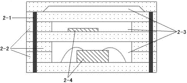
[0024] On the basis of the specific embodiment 1, including the support layer 2-2, a blind cavity structure 2-3 is formed between the support layer and the upper and lower layers of the support layer, so as to realize the chip and / or passive components (such as filters) 3-5, resistors 3-6 and capacitors, etc.) are embedded. In this specific embodiment, the control unit layer 3-2 and the power unit layer 3-4 are integrated into chips by gold wire bonding and flip-chip welding.

specific Embodiment 3

[0025] On the basis of specific embodiment 1 or 2, according to the circuit characteristics of each layer of thin film ceramic circuit, the base material of each layer of thin film ceramic circuit substrate is set. According to the circuit characteristics of each layer of thin film ceramic circuit, the base material of each layer of thin film ceramic circuit substrate can be set, such as the radio frequency filter unit layer 3-3 adopts ferrite base material (in this specific embodiment, the dielectric constant is greater than or equal to 20, less than or equal to 40 high-dielectric ferrite), the control unit layer 3-2 is made of alumina substrate, and the power unit layer 3-4 is made of aluminum nitride substrate; in this way, each layer of thin film ceramic circuit substrate can use different The base material realizes the optimized combination of the structural properties of each layer. The substrates selected for the multiple unit layers in this specific embodiment are just...


PUM


Abstract

The invention provides a three-dimensional stack structure of a thin-film ceramic circuit. Between two adjacent thin-film ceramic substrates, through ball mounting welding or prefabricated pad welding, stacking of more than three thin-film ceramic circuit substrates is realized. Solid metal through holes are used for realizing electric connection of a random layer. The structure comprises a local electromagnetic self-shielding structure of a chip and/or a passive component. The local electromagnetic self-shielding structure comprises an upper metal layer, a lower metal layer and side surface solid metal through holes. The three-dimensional stack structure can realize stacking of the thin-film ceramic circuit so that an active chip, an RF structure, a high-power structure, a broadband switching structure and the like are integrally integrated in a three-dimensional direction, thereby reducing plan area of a function core by more than 70%, effectively improving product integration level, synchronously realizing hermetic sealing and electromagnetic self-shielding, and improving product adaptability. The three-dimensional stack structure can replace 60-70% of similar products and has advantages of saving cost by more than 60% and improving production efficiency by more than 40%.

Description

technical field [0001] The invention relates to a three-dimensional stacked structure of a thin film ceramic circuit, in particular to a three-dimensional stacked structure of a thin film ceramic circuit in the field of integration of passive components. Background technique [0002] The existing high-density integration process mainly adopts multi-chip assembly (SIP) technology, which assembles chips such as MMIC / ASIC and micro-chip components on LTCC or multi-layer PCB substrates, and uses gold wire bonding to realize components and components. Cascading of multifunctional substrates. Its shortcomings mainly lie in: on the one hand, all functional units are tiled and installed in the two-dimensional direction of the substrate, the interconnection design of embedded devices is relatively complicated, the product is large in size, high in cost, and it is not convenient for independent testing; on the other hand, LTCC Or the PCB substrate process has great limitations in ter...

Claims


Application Information

Patent Timeline
Patent Type & Authority Applications(China)
IPC IPC(8): H01L25/07H01L23/31H01L23/60
CPCH01L23/3128H01L23/60H01L25/071H01L2224/16225H01L2224/48091H01L2224/48227H01L2924/16152H01L2924/00014
Inventor 秦跃利王春富李彦睿
Owner SOUTHWEST CHINA RES INST OF ELECTRONICS EQUIP
Why Eureka
Try Eureka