Fan-out package structure and preparation method thereof
A packaging structure, fan-out technology, applied in semiconductor/solid-state device manufacturing, electrical components, electrical solid-state devices, etc., can solve problems such as damage to electronic components, cracking of semiconductor chips, and affecting the handling of semiconductor equipment, so as to avoid warping, Avoid the effect of cracking
- Summary
- Abstract
- Description
- Claims
- Application Information
AI Technical Summary
Problems solved by technology
Method used
Image
Examples
Embodiment 1
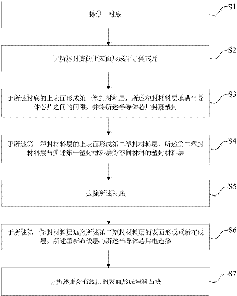
[0062] see figure 1 , this embodiment provides a method for preparing a fan-out packaging structure, the method for preparing a fan-out packaging structure includes the following steps:
[0063] 1) providing a substrate;
[0064] 2) forming a semiconductor chip on the upper surface of the substrate;
[0065] 3) forming a first plastic packaging material layer on the upper surface of the substrate, the first plastic packaging material layer fills the gap between the semiconductor chips, and encapsulates the semiconductor chips;
[0066] 4) forming a second molding material layer on the upper surface of the first molding material layer, wherein the second molding material layer and the first molding material layer are molding material layers of different materials;
[0067] 5) removing the substrate;
[0068] 6) forming a rewiring layer on the surface of the first molding material layer away from the second molding material layer, and the rewiring layer is electrically connec...
Embodiment 2
[0110] read on Figure 9 , this embodiment also provides a fan-out packaging structure, the fan-out packaging structure is prepared by the preparation method described in the first embodiment, the fan-out packaging structure includes: a rewiring layer 16, the The rewiring layer 16 includes opposite first surfaces and second surfaces; the semiconductor chip 13 is located on the first surface of the rewiring layer 16 and is electrically connected to the rewiring layer 16; the first plastic encapsulation material Layer 14, the first molding material layer 14 is located on the first surface of the rewiring layer 16, the first molding material layer 14 fills the gaps between the semiconductor chips 13, and the semiconductor chips 13 encapsulating plastic packaging; the second plastic packaging material layer 15, the second plastic packaging material layer 15 is located on the surface of the first plastic packaging material layer 14 away from the rewiring layer 16, the second plasti...
PUM
 Abstract
Description
Claims
Application Information


