

Organic light emitting display panel, display device thereof and manufacturing method thereof
A technology of light-emitting display and manufacturing method, which is applied in the manufacturing/processing of organic light-emitting devices, organic light-emitting devices, semiconductor/solid-state device manufacturing, etc., can solve the problems of poor adhesion and easy peeling, and achieve enhanced adhesion , to avoid the effect of peeling phenomenon
- Summary
- Abstract
- Description
- Claims
- Application Information
AI Technical Summary
Problems solved by technology
Method used
Image

Examples
experiment example 1
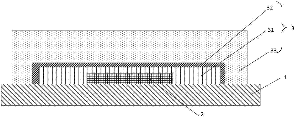
[0125] Experimental example 1, using the method of the embodiment of the present invention, using atomic layer deposition to prepare Al 2 o 3 is the first inorganic layer of the material (thickness is 50nm), TMA is used as the precursor of the transition layer to prepare a monomolecular layer transition layer, and inkjet printing is used to deposit polymethyl methacrylate (PMMA) as the first organic layer (thickness is 10 μm ), prepared as figure 1 The organic light-emitting display panel shown.
experiment example 2
[0126] Experimental example 2, using the method of the embodiment of the present invention, using atomic layer deposition to prepare Al 2 o 3 is the first inorganic layer of the material (thickness is 50nm), using HMDS as the precursor of the transition layer to prepare a monomolecular layer transition layer, using inkjet printing to deposit polymethyl methacrylate (PMMA) as the first organic layer (thickness is 10 μm ), prepared as figure 1 The organic light-emitting display panel shown.
experiment example 3
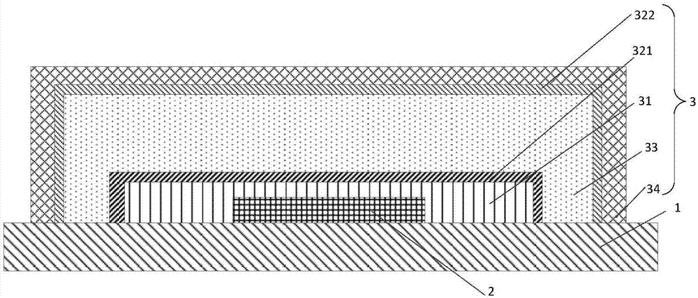
[0127] Experimental example 3, using the method of the embodiment of the present invention, using atomic layer deposition to prepare Al 2 o 3 The first inorganic layer (thickness is 30nm) of the material, TMA is used as the precursor of the transition layer to prepare a monomolecular layer transition layer, and inkjet printing is used to deposit polymethyl methacrylate (PMMA) as the first organic layer (thickness is 10 μm ), and then prepared Al by atomic layer deposition 2 o 3 Be the second inorganic layer of material (thickness is 30nm), prepare as figure 2 The organic light-emitting display panel shown.
PUM
 Abstract
Description
Claims
Application Information