Array substrate and manufacturing method therefor and display apparatus

A fabrication method and array substrate technology are applied in the fabrication of array substrates, in the fields of array substrates and display devices, and can solve the problems of lowering product yield by photolithography process and complex fabrication process of TFT substrates, etc.

Active Publication Date: 2017-11-03
SHANGHAI TIANMA MICRO ELECTRONICS CO LTD
View PDF2 Cites 14 Cited by
  • Summary
  • Abstract
  • Description
  • Claims
  • Application Information

AI Technical Summary

Problems solved by technology

[0007] The object of the present invention is to provide a method for manufacturing an array substrate, an array substrate and a display device, which are used to solve the problem that the existing TFT substrate manufacturing process is relatively complicated, and generally requires seven photolithography processes. At present, there is an urgent need for an effective way to reduce The photolithography process will not reduce the problem of product yield

Method used


Image

  • Array substrate and manufacturing method therefor and display apparatus
  • Array substrate and manufacturing method therefor and display apparatus
  • Array substrate and manufacturing method therefor and display apparatus

Examples


Embodiment 1

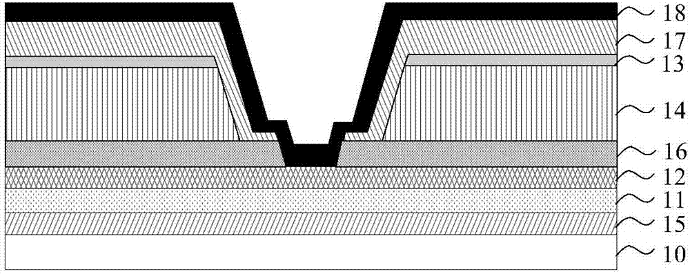
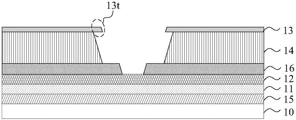
[0058] Embodiment 1: a process flow of forming a first through hole in a display area on an array substrate.

[0059] In a specific implementation, the array substrate has at least two structures, the first structure and the second structure. Since the array substrate of the first structure and the array substrate of the second structure above, the main difference between the two lies in the first electrode layer and the second structure. Is the second electrode layer a pixel electrode or a common electrode, and in the display area, the first through hole is used to connect the pixel electrode and the source-drain metal layer, so the array substrate of the first structure and the array of the second structure In the substrate, the pattern of the first electrode layer and the pattern of the second electrode layer are different to some extent, but the other film layers, and the order and pattern of making each film layer are the same, and the manufacturing process is also basical...

Embodiment 2

[0108] Embodiment 2: a process flow of forming a second through hole in the display area on the array substrate.

[0109] In specific implementation, the same as the first embodiment above, the second embodiment also introduces the structure of forming the second through hole in the display area on the array substrate of the first structure and the array substrate of the second structure respectively. . Since the array substrate of the first structure and the array substrate of the second structure have a certain difference between the first electrode layer pattern and the second electrode layer pattern, and the other film layers and the manufacturing sequence of each film layer and The patterns and the like are the same, and the manufacturing process is also basically the same, therefore, the formation of the second through hole will not be described too much here. The difference in structure between the array substrate of the first structure and the array substrate of the s...

Embodiment 3

[0147] Embodiment 3: the process flow of forming the first through hole and the second through hole in the non-display area on the array substrate.

[0148]In a specific implementation, in the non-display area of ​​the array substrate, whether it is the array substrate of the first structure or the array substrate of the second structure, the structures of the first through holes and the second through holes formed are the same. In addition, the first through hole and the second through hole may be arranged in the bonding area, and the specific manufacturing process flow is similar to that of Embodiment 1 and Embodiment 2, and reference may be made to the above two embodiments.

[0149] Such as Figure 21a As shown, it is a top view of the first through hole formed in the non-display area of ​​the array substrate provided by the embodiment of the present invention; Figure 21b Shown, provided for the embodiment of the present invention Figure 21a Schematic diagram of the cr...


PUM


Abstract

The invention relates to an array substrate and a manufacturing method therefor and a display apparatus, and aims to solve the problem of a relatively complex manufacturing process of a TFT substrate, so that an effective mode for reducing photolithography techniques without lowering product yield is needed urgently. The manufacturing method comprises the steps of forming a gate metal layer pattern, a gate insulating layer thin film, an active layer pattern and source and drain metal layer patterns on a substrate; forming a planarization layer thin film, a first electrode layer pattern, a first insulating layer thin film and a photoresist pattern on the source and drain metal layer patterns in sequence; performing a dry etching process on the first insulating layer thin film and the planarization layer thin film in sequence, wherein via holes formed in the first insulating layer thin film, a first shielding electrode and the planarization layer thin film form a first through hole; and forming a second electrode layer pattern which comprises a first bridging electrode on the first insulating layer thin film, and enabling the first bridging electrode to at least fully cover the first through hole region and to be connected with the source and drain metal layer patterns.

Description

technical field [0001] The present invention relates to the technical field of array substrates, in particular to a method for manufacturing an array substrate, an array substrate and a display device. Background technique [0002] At present, in the manufacture of liquid crystal display panels, especially in the process of manufacturing TFT (Thin Film Transistor, thin film transistor) substrates, the manufacturing process is relatively complicated, and generally seven photolithography processes are required, which are gate, active layer, source Drain, planarization layer, first passivation layer, via hole and pixel electrode; or, gate, active layer & source drain, first passivation layer, planarization layer, common electrode, via hole and pixel electrode. Multiple mask exposures not only increase the process time and production cost, but also increase the difficulty of the process, which is prone to defects caused by insufficient alignment accuracy and reduces the product...

Claims


Application Information

Patent Timeline
IPC IPC(8): H01L21/84H01L27/12
CPCH01L27/1214H01L27/124H01L27/1259H01L27/1288
Inventor 戴文君
Owner SHANGHAI TIANMA MICRO ELECTRONICS CO LTD
Why Eureka
Try Eureka