Array substrate and liquid crystal display panel

An array substrate and array technology, applied in nonlinear optics, instruments, optics, etc., can solve the problems of dark stripes shifting pixel centers, poor alignment, etc., and achieve the effect of improving quality and improving poor alignment

Active Publication Date: 2017-11-07
SHENZHEN CHINA STAR OPTOELECTRONICS TECH CO LTD
View PDF7 Cites 12 Cited by
  • Summary
  • Abstract
  • Description
  • Claims
  • Application Information

AI Technical Summary

Problems solved by technology

For COA products, the color resist layer is designed on the side of the Array substrate, such as figure 1 As shown, in order to make the ITO pixel electrode 110 conduct with the drain 310 through the via hole (Via hole) 210, the color resistance layer 400 will be dug at the via hole 210 to form a color resistance opening (CF open) 410 , and if figure 2 As shown, the thickness of the color-resist layer 400 is usually about 3um. Compared with the ITO pixel electrode 110 with a thickness of 0.04um, the thickness diff

Method used


Image

  • Array substrate and liquid crystal display panel
  • Array substrate and liquid crystal display panel
  • Array substrate and liquid crystal display panel

Examples


Embodiment Construction

[0027] In order to further illustrate the technical means adopted by the present invention and its effects, the following describes in detail in conjunction with preferred embodiments of the present invention and accompanying drawings.

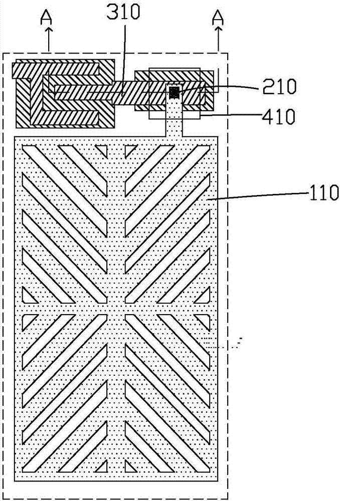
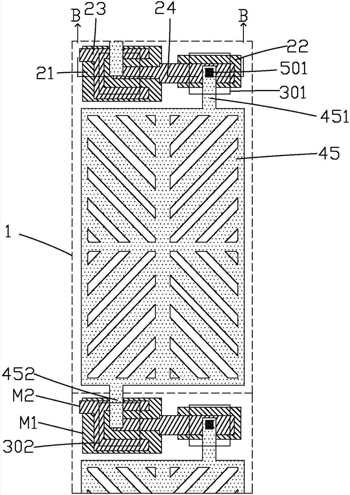
[0028] The present invention firstly provides an array substrate, please refer to image 3 and Figure 4 , the first embodiment of the array substrate of the present invention includes a plurality of gate lines (not shown) and a plurality of data lines (not shown) intersecting the plurality of gate lines, and the plurality of A plurality of pixel units 1 arranged in an array are defined by the plurality of gate lines and the plurality of data lines.

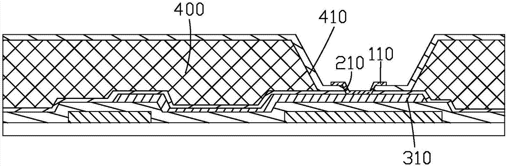
[0029] Specifically, the array substrate includes a base substrate 10, a first metal layer M1 disposed on the base substrate 10, an insulating layer 20, a second metal layer M2, a first spacer layer 50, and a first metal layer M1 disposed on the first metal layer. The color resist layer 30 on a...


PUM


Abstract

The invention provides an array substrate and a liquid crystal display panel. The array substrate comprises multiple pixel units in array arrangement. Each pixel unit comprises a substrate, a thin film transistor, a color resistance layer and a pixel electrode, the shape of each pixel electrode is in central symmetry, each pixel electrode comprises a connection protruding block contacting with a drain electrode to realize connection and a symmetric protruding block in central symmetry with the connection protruding block, and a first color resistance opening and a second color resistance opening corresponding to the connection protruding block and the symmetric protruding block respectively are formed in the color resistance layer. Therefore, poor matching of existing COA-type array substrates caused by the fact that color resistance opening and pixel electrode design is asymmetric can be improved, and quality of the liquid crystal display panel can be improved effectively.

Description

technical field [0001] The invention relates to the field of display technology, in particular to an array substrate and a liquid crystal display panel. Background technique [0002] A liquid crystal display (Liquid Crystal Display, LCD) has many advantages such as a thin body, power saving, and no radiation, and has been widely used. Such as: LCD TV, mobile phone, personal digital assistant (PDA), digital camera, computer screen or laptop screen, etc. [0003] Generally, a liquid crystal display device includes a housing, a liquid crystal panel disposed in the housing, and a backlight module disposed in the housing. Among them, the structure of the liquid crystal panel is mainly composed of a thin film transistor array (Thin Film Transistor Array, TFT Array) substrate, a color filter (Color Filter, CF) substrate, and a liquid crystal layer (Liquid Crystal Layer) arranged between the two substrates. Its working principle is to control the rotation of the liquid crystal mol...

Claims


Application Information

Patent Timeline
IPC IPC(8): G02F1/1335G02F1/1343G02F1/1362
CPCG02F1/133514G02F1/134309G02F1/1362G02F1/136222
Inventor 安立扬
Owner SHENZHEN CHINA STAR OPTOELECTRONICS TECH CO LTD
Why Eureka
Try Eureka