
Light-emitting diode (LED) epitaxial structure, manufacturing method thereof, and LED

A technology of light-emitting diodes and epitaxial structures, which is applied in the direction of electrical components, circuits, semiconductor devices, etc., can solve problems such as device failure, achieve good crystal quality, and solve the effect of device failure

Active Publication Date: 2017-11-07
厦门未来显示技术研究院有限公司
View PDF3 Cites 3 Cited by
  • Summary
  • Abstract
  • Description
  • Claims
  • Application Information

AI Technical Summary

Problems solved by technology

[0006] In view of this, the present invention provides a light-emitting diode epitaxial structure and its manufacturing method, and a light-emitting diode to solve the problem of device failure caused by leakage due to insufficient filling of V-shaped pits in the prior art

Method used


Image

  • Light-emitting diode (LED) epitaxial structure, manufacturing method thereof, and LED
  • Light-emitting diode (LED) epitaxial structure, manufacturing method thereof, and LED
  • Light-emitting diode (LED) epitaxial structure, manufacturing method thereof, and LED

Examples


Embodiment Construction

[0038] As mentioned in the background section, in the prior art, in order to improve the problem of extremely weak luminescence of other quantum wells in the p-type GaN layer in the multiquantum wells, a V-Pits structure is introduced into the multiquantum wells. However, the introduction of the V-Pits structure is likely to cause the problem that the V-shaped pits of the multi-quantum wells are not filled enough to cause leakage and cause device failure.

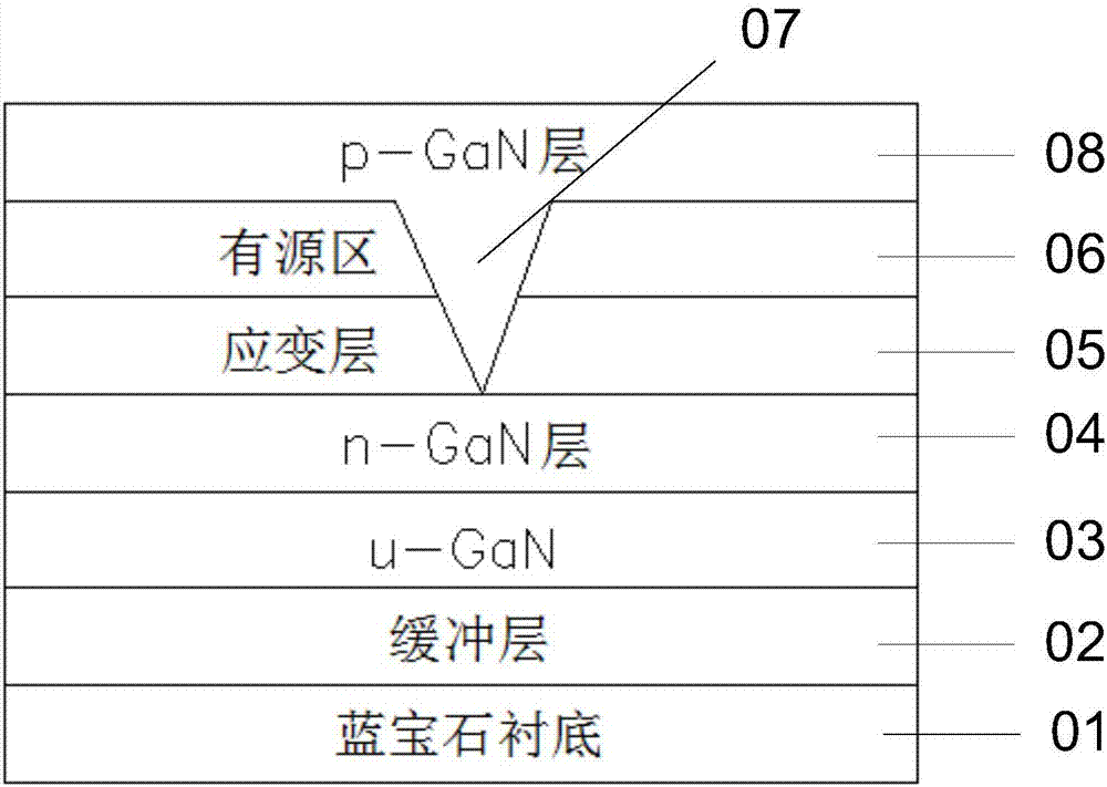
[0039] The inventors found that the reason for the above phenomenon is that the light-emitting diode epitaxial structure in the prior art is such as figure 1 As shown, the manufacturing process is: growing buffer layer 02, u-GaN layer 03, n-GaN layer 04, strain layer 05, active region 06, p-GaN layer 08 on sapphire substrate 01; among them, the V-shaped pit (V-Pits) 07 are formed in the strained layer 05 and are longer than the active region 06 , and finally the p-GaN layer 08 slowly fills up the V-shaped pits 07 . When gr...


PUM

PropertyMeasurementUnit
thicknessaaaaaaaaaa
heightaaaaaaaaaa

Abstract

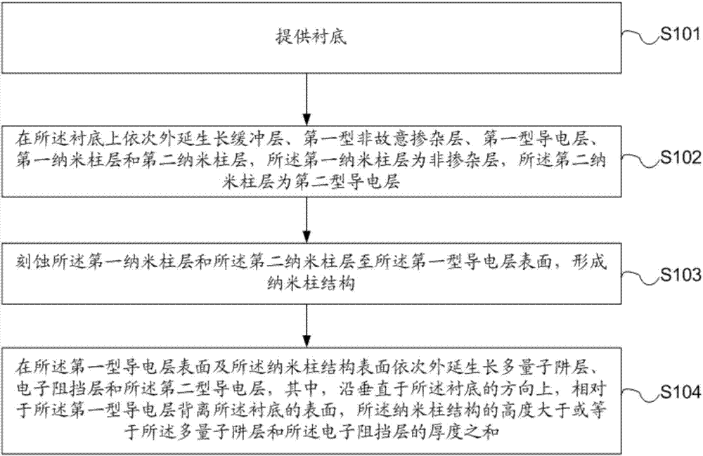
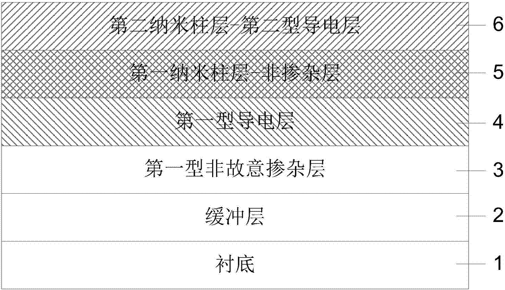
The application provides a light-emitting diode (LED) epitaxial structure, a manufacturing method thereof, and an LED. The manufacturing method of the LED epitaxial structure includes: providing a substrate; successively and epitaxially growing a buffer layer, a first type of unintentional doping Layer, a first type of conductive layer, an non-doped layer and a second type of conductive layer on the substrate; etching the non-doped layer and the second type of conductive layer to form a nano-pillar structure; and re-epitaxially growing a multi-quantum well layer, an electron blocking layer, and a second type of conductive layer. The nano-pillar structure replaces a conventional V-pits structure. Because the nano-pillar structure has good crystal quality and the first type of conductive layer can be isolated from the second type of conductive layer, device failure caused by electric leakage of the V-pits structure can be solved.

Description

technical field [0001] The invention relates to the technical field of optoelectronic devices, in particular to an epitaxial structure of a light emitting diode, a manufacturing method thereof, and a light emitting diode. Background technique [0002] Light Emitting Diode (LED) is called the fourth generation lighting source or green light source. It has the characteristics of energy saving, environmental protection, long life and small size. It is widely used in various indications, displays, decorations, backlights, and general lighting. and city night scenes. [0003] Light-emitting diodes are usually composed of III-IV semiconductor compounds. Most of the blue-green light-emitting diodes are epitaxial multi-layer gallium nitride-based material films on the substrate to form a PN junction, and electrons and holes recombine in the active region to emit light. The luminous efficiency of light-emitting diodes is closely related to the internal quantum efficiency, and the in...

Claims


Application Information

Patent Timeline
Patent Type & Authority Applications(China)
IPC IPC(8): H01L33/00H01L33/02H01L33/06H01L33/14H01L33/22
CPCH01L33/0075H01L33/02H01L33/06H01L33/145H01L33/22
Inventor 林志伟陈凯轩李俊贤卓祥景汪洋
Owner 厦门未来显示技术研究院有限公司
Learn More