Fabrication method of vertical double-diffused metal-oxide-semiconductor (VDMOS) device

A device and gate oxide technology, applied in the field of VDMOS device fabrication, can solve the problems of increasing VDMOS device fabrication cost and complex fabrication process, etc.

Inactive Publication Date: 2017-11-10
PEKING UNIV FOUNDER GRP CO LTD +1
View PDF4 Cites 2 Cited by
  • Summary
  • Abstract
  • Description
  • Claims
  • Application Information

AI Technical Summary

Problems solved by technology

[0005] The embodiment of the present invention provides a method for manufacturing a VDMOS device, which solves the problem that multiple repeated manufacturing steps are required when making a VDMOS device in the prior art, which complicates the manufacturing process and increases the manufacturing cost of the VDMOS device.

Method used


Image

  • Fabrication method of vertical double-diffused metal-oxide-semiconductor (VDMOS) device
  • Fabrication method of vertical double-diffused metal-oxide-semiconductor (VDMOS) device
  • Fabrication method of vertical double-diffused metal-oxide-semiconductor (VDMOS) device

Examples


Embodiment Construction

[0045] In order to make the purpose, technical solutions and advantages of the embodiments of the present invention clearer, the technical solutions in the embodiments of the present invention will be clearly and completely described below in conjunction with the drawings in the embodiments of the present invention. Obviously, the described embodiments It is a part of embodiments of the present invention, but not all embodiments. Based on the embodiments of the present invention, all other embodiments obtained by persons of ordinary skill in the art without making creative efforts belong to the protection scope of the present invention.

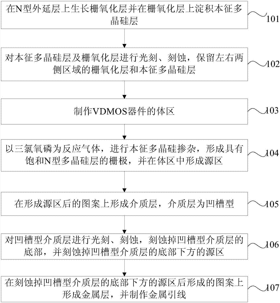
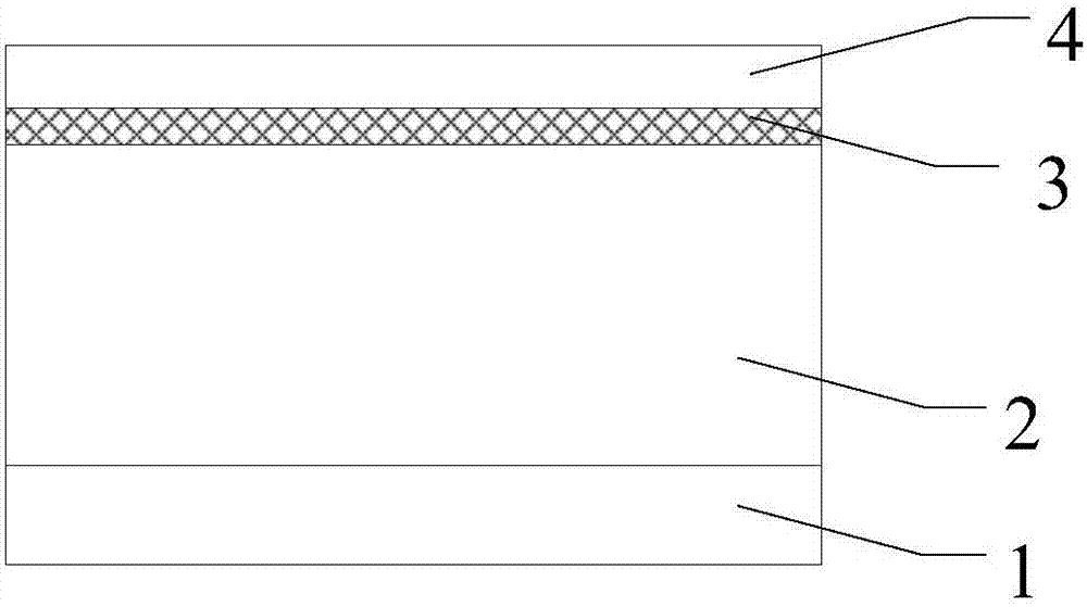
[0046] figure 1 It is a flow chart of Embodiment 1 of the manufacturing method of the VDMOS device of the present invention, such as figure 1 As shown, the manufacturing method of the VDMOS device provided in this embodiment includes the following steps.

[0047] Step 101 , growing a gate oxide layer 3 on the N-type epitaxial layer 2 and ...


PUM


Abstract

The invention provides a fabrication method of a vertical double-diffused metal-oxide-semiconductor (VDMOS) device. The method comprises the steps of growing a grid oxide layer on an N-type epitaxial layer, and depositing an intrinsic poly-silicon layer on the grid oxide layer; photoetching and etching the intrinsic poly-silicon layer and the grid oxide layer, and reserving the grid oxide layer and the intrinsic poly-silicon layer on a left-side region and a right-side region; fabricating a body region of the VDMOS device; performing intrinsic poly-silicon doping by taking POCl3 as a reaction gas to form a grid with a saturated poly-silicon layer, and forming a source region in the body region; forming a dielectric layer on a pattern after the source region is formed, wherein the dielectric layer is in a groove shape; photoetching and etching the groove-shaped dielectric layer to etch a bottom part of the groove-shaped dielectric layer, and etching the source region below the bottom part of the groove-shaped dielectric layer; and forming a metal layer on a pattern formed after the source region below the bottom part of the groove-shaped dielectric layer is etched, and fabricating a metal lead. By the fabrication method, high performance of the VDMOS device is ensured.

Description

technical field [0001] Embodiments of the present invention relate to the technical field of semiconductor manufacturing, and in particular to a method for manufacturing a VDMOS device. Background technique [0002] A single vertical double diffused metal-oxide semiconductor transistor (abbreviation: VDMOS) has both the advantages of a bipolar transistor and an ordinary MOS device. Regardless of switching or linear applications, VDMOS is an ideal power device. VDMOS devices are mainly used in motor speed regulation, inverters, uninterruptible power supplies, electronic switches, hi-fi audio, automotive electrical appliances and electronic ballasts. VDMOS devices are divided into enhanced VDMOS devices and depletion VDMOS devices. [0003] Figure 11 is a schematic cross-sectional structure diagram of a VDMOS device in the prior art, Figure 12 For the production flow chart of VDMOS device in the prior art, as Figure 11 and Figure 12 As shown, the existing VDMOS device ...

Claims


Application Information

Patent Timeline
Patent Type & Authority Applications(China)
IPC IPC(8): H01L21/336
CPCH01L29/66734
Inventor 赵圣哲
Owner PEKING UNIV FOUNDER GRP CO LTD
Why Eureka
Try Eureka