Device for eliminating high electric field

A high electric field and device technology, applied in electrical components, semiconductor devices, circuits, etc., can solve problems such as device breakdown, affecting device withstand voltage, and charge imbalance, so as to improve breakdown voltage, increase current capability, reduce The effect of small channel resistance

Active Publication Date: 2017-11-17
UNIV OF ELECTRONICS SCI & TECH OF CHINA
View PDF7 Cites 2 Cited by
  • Summary
  • Abstract
  • Description
  • Claims
  • Application Information

AI Technical Summary

Problems solved by technology

However, in actual device manufacturing, due to various reasons, the charge imbalance between P and N bars is easy to generate a high electric field, especially at the edge of the superjunction structure, which causes premature breakdown of the device and affects the withstand voltage of the device.

Method used


Image

  • Device for eliminating high electric field
  • Device for eliminating high electric field
  • Device for eliminating high electric field

Examples


Embodiment 1

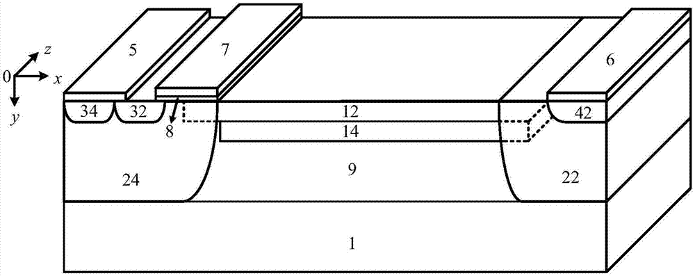
[0032] Such as figure 1As shown, a device for eliminating high electric fields is characterized in that its cell structure includes a substrate 1, a source contact electrode 5, a drain contact electrode 6, a gate electrode 7, a gate oxide layer 8, and a second type drift region 9. Second type strips 12, first type strips 14, second type buffer regions 22, first type well regions 24, second type heavily doped regions 32, first type heavily doped regions 34, third type heavily doped regions doping region 42; the second type drift region 9 is arranged on the upper surface of the substrate 1; the first type well region 24 is embedded and arranged on the left side of the second type drift region 9, and its upper surface is connected with the second type The upper surface of the drift region 9 is connected; the second type buffer region 22 is embedded on the right side of the second type N-type drift region 9, and its upper surface is connected with the upper surface of the second t...

Embodiment 2

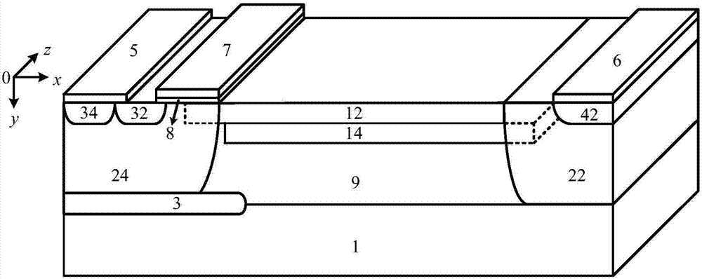
[0034] Such as figure 2 As shown, this embodiment is basically the same as Embodiment 1, the difference is that: under the first type well region 24, the left end of the junction of the substrate 1 and the second type drift region 9 is introduced into the first type buried layer 3, and its upper surface The first type well region 24 is partially embedded, and the lower surface is partially embedded in the substrate 1; thereby preventing the first type well region 24 from communicating with the substrate 1, thereby improving the stability of the device.

Embodiment 3

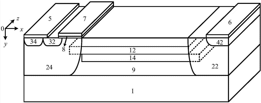
[0036] Such as image 3 As shown, the present embodiment is basically the same as Embodiment 1, the difference is that the second type bar 12 and the first type bar 14 are arranged in the body of the second type drift region 9, and the upper surface thereof is not in contact with the upper surface of the second type drift region 9. The surface is connected, and the lower surface is not connected with the lower surface of the second type drift region 9 .


PUM


Abstract

The invention provides a device for eliminating a high electric field. A cellular structure comprises a substrate, a source contact electrode, a drain contact electrode, a grid electrode, a grid oxide layer, a second type drift region, a second type bar, a first type bar, a second type buffer region, a first type well region, a second type heavy-doped region, a first type heavy-doped region and a third type heavy-doped region. According to the device for eliminating the high electric field, the left end of the second type bar extends into the first type well and is not connected with the second type heavy-doped region; the right end of the first type bar extends into the second type buffer region, so that the second type bar at the left end is exhausted by a multi-surface first type impurity, and the first type bar at the right end is exhausted by a multi-surface second type impurity; therefore, the peak of an electric field at a super junction edge is weakened, in-advance breakdown of the device is avoided, and the breakdown voltage of a super junction device is further increased; and the left side of the second type bar extends into the first type well region, so that the channel resistance of the device in an on state is reduced, and the specific on-state resistance of the device is reduced.

Description

technical field [0001] The invention belongs to the technical field of semiconductor power devices, and in particular relates to a device for eliminating high electric fields. Background technique [0002] The development of modern power electronics technology requires power devices to have superior high-voltage, high-speed, and low-power performance. In order to meet high withstand voltage, traditional power MOSFETs need to reduce the concentration of the drift region or increase the length of the drift region, but this approach will make the conduction The resistance also increases accordingly. Therefore, in traditional power device applications, on-resistance and breakdown voltage are contradictory, and the limit relationship between them is R on ∝BV 2.5 . Superjunction (SJ) devices, as a new type of power device, have the advantage of greatly reducing the specific on-resistance of the device while keeping the withstand voltage of the device basically unchanged. In su...

Claims


Application Information

Patent Timeline
Patent Type & Authority Applications(China)
IPC IPC(8): H01L29/06H01L29/739H01L29/78
CPCH01L29/0634H01L29/7393H01L29/7394H01L29/7823H01L29/7816H01L29/7813H01L29/0878
Inventor 章文通詹珍雅李珂余洋梁龙飞乔明张波
Owner UNIV OF ELECTRONICS SCI & TECH OF CHINA
Why Eureka
Try Eureka