Large-scale MIMO antenna structure and manufacturing process

A large-scale, antenna technology, applied in the field of massive MIMO antenna structure and manufacturing process, can solve the problems of difficult control of relative displacement and spacing, low welding reliability, etc., to achieve the effect of reducing mass, simplifying assembly steps, and ensuring reliability

Pending Publication Date: 2017-11-24
ZHONGTIAN BROADBAND TECH +1
View PDF0 Cites 15 Cited by
  • Summary
  • Abstract
  • Description
  • Claims
  • Application Information

AI Technical Summary

Problems solved by technology

SMT is generally only used for one-layer placement. For multi-layer placement, the relative displacement and spacing between layers are difficult to control; when large-area bonding, internal welding reliability is low

Method used


Image

  • Large-scale MIMO antenna structure and manufacturing process
  • Large-scale MIMO antenna structure and manufacturing process
  • Large-scale MIMO antenna structure and manufacturing process

Examples


Embodiment Construction

[0027] In order to make the technical means realized by the present invention clear, the present invention will be further described below in conjunction with the accompanying drawings.

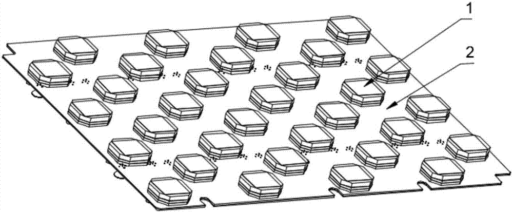
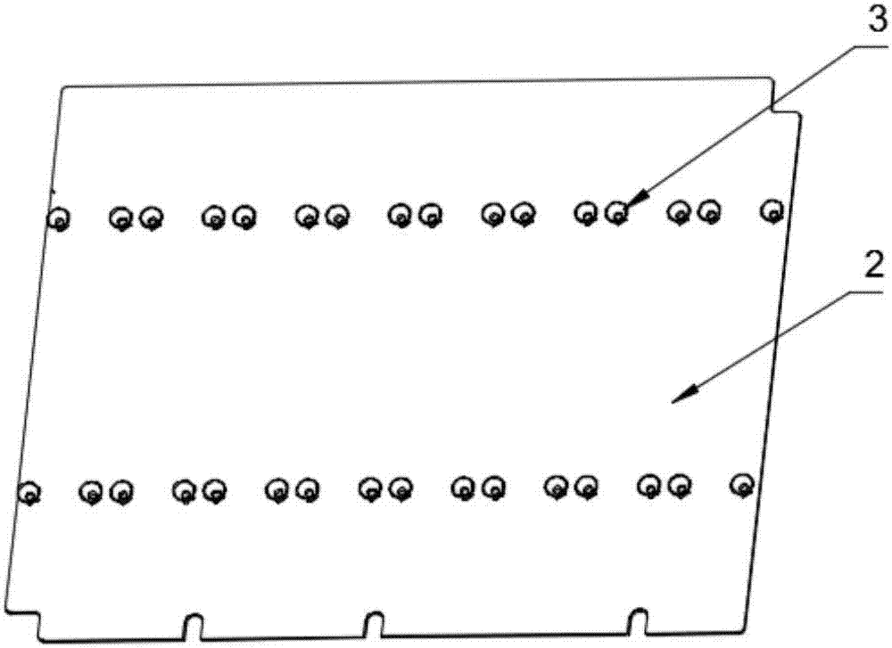
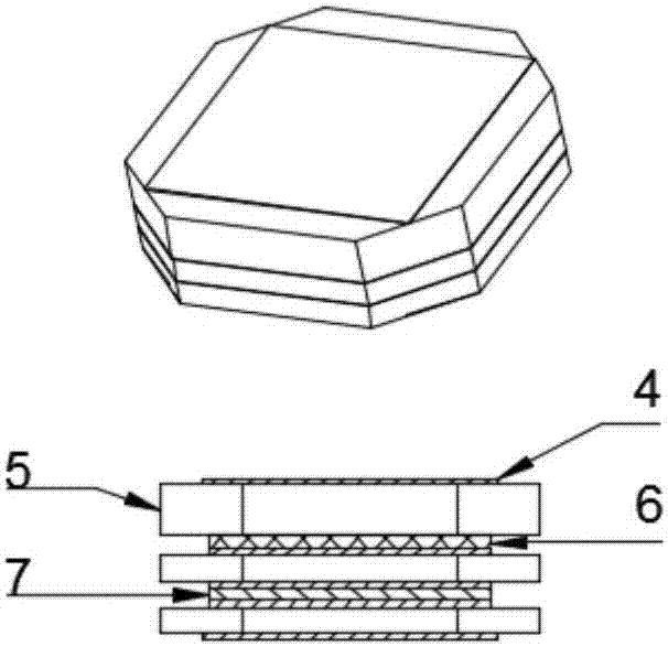
[0028] like Figure 1 to Figure 6 As shown, a large-scale MIMO antenna structure includes a PCB substrate 2 and N×N antenna units 1; the PCB substrate 2 includes two layers of PCB substrate dielectric boards 12, and the interlayer formed by the two layers of PCB substrate dielectric boards is In the middle layer, the metal is laid on the upper surface 13 of the PCB substrate, the metal is laid on the lower surface 16 of the PCB substrate, and the transmission line structure is laid on the middle layer. The transmission line structure includes the middle layer metal signal line 14 and the middle layer metal ground 15, which penetrate the two layers of PCB substrate media A plurality of metallized via holes 11 of the board 12 communicate with the metal laid on the upper surface 13 of the PCB su...


PUM


Abstract

The invention discloses a large-scale MIMO antenna structure and manufacturing process, which includes a plurality of antenna units arranged in an array, each antenna unit is composed of three or more layers of dielectric boards; the PCB substrate is two layers of dielectric boards and The structure of the three-layer metal layer combines the power division network and the calibration network on the transmission line structure of the middle metal layer, and the upper and lower conductive metals are grounded; each antenna unit is connected to the substrate through a metal probe for feeding; the antenna unit adopts SMT technology directly Solder to the corresponding antenna unit pad on the substrate, the accuracy is guaranteed by welding, and no adjustment is required. The invention has low profile, compact structure, high integration, light weight, only a few assembly steps, high production efficiency, and can ensure high consistency and stability.

Description

[technical field] [0001] The invention mainly relates to the field of antenna design and the field of SMT process flow, and in particular to a massive MIMO antenna structure and manufacturing process. [Background technique] [0002] Multi-antenna transmission and reception technology, that is, MIMO technology, can be roughly divided into two categories: transmit / receive diversity and space multiplexing. Traditionally, multiple antennas are used to increase diversity to overcome channel fading. Signals with the same information are sent out through different paths, and information conforming to multiple independent fadings can be obtained at the receiver, thereby obtaining higher reception reliability. In the existing massive MIMO antenna, the power division network and the calibration network need to be implemented separately on two PCB boards. Metal spacers are required between the antenna units, which increases the overall weight and cost of the antenna, and the connectio...

Claims


Application Information

Patent Timeline
Patent Type & Authority Applications(China)
IPC IPC(8): H01Q1/36H01Q1/38H01Q1/50H01Q21/00H01Q21/06
CPCH01Q1/36H01Q1/38H01Q1/50H01Q21/0006H01Q21/0087H01Q21/065
Inventor 葛磊刘文达赵田野
Owner ZHONGTIAN BROADBAND TECH
Why Eureka
Try Eureka