Startup circuit

A technology of startup circuit and voltage control circuit, which is applied in the direction of adjusting electrical variables, control/regulating systems, instruments, etc., can solve the problems of large chip area and long startup time of startup circuit, and achieves a small chip area and improves startup time. Effect

Active Publication Date: 2017-11-28
上海韦玏微电子有限公司 +1
View PDF6 Cites 3 Cited by
  • Summary
  • Abstract
  • Description
  • Claims
  • Application Information

AI Technical Summary

Problems solved by technology

[0003] The technical problem to be solved by the present invention is to provide a startup circuit that occupies a small chip area and can improve the startup time in order to overcome the disadvantages of the startup circuit of the reference voltage source in the prior art that the startup time is too long and occupies a large chip area

Method used


Image

  • Startup circuit
  • Startup circuit
  • Startup circuit

Examples


Embodiment 1

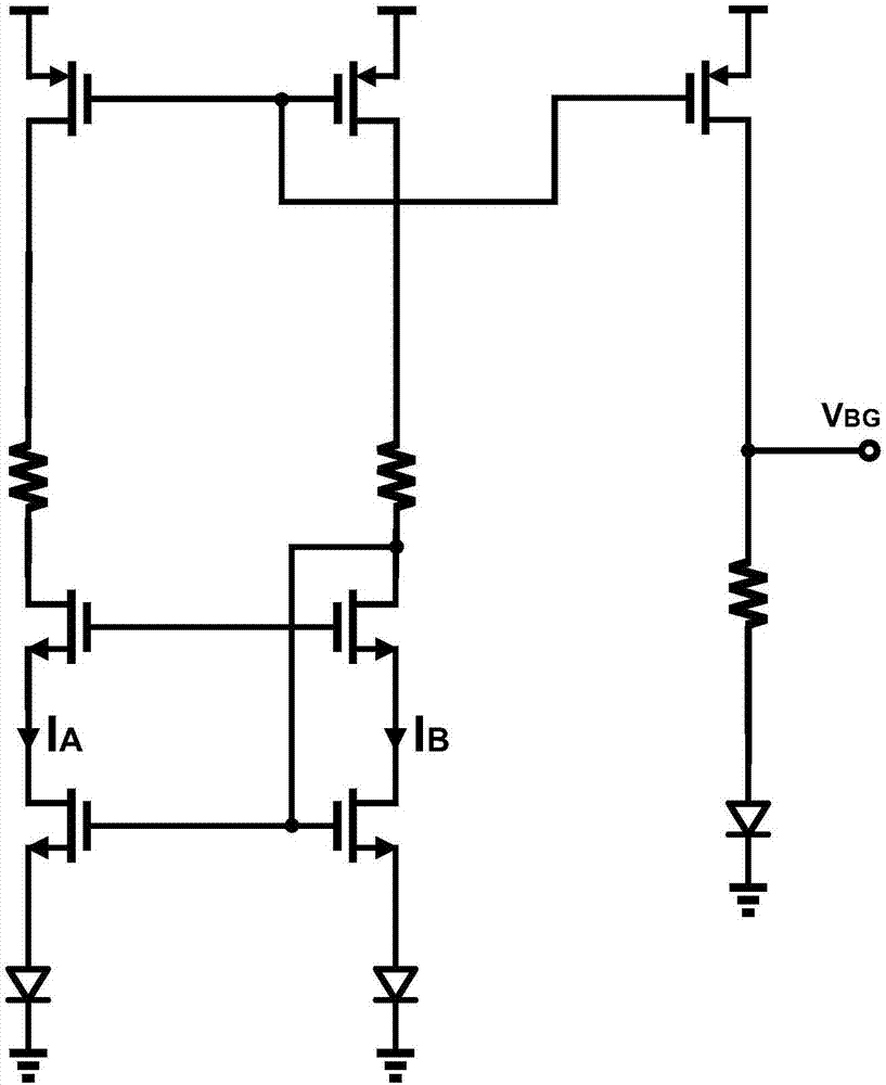
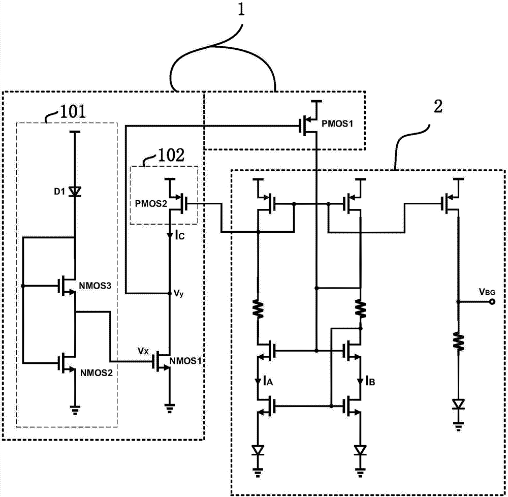
[0028] Such as image 3 As shown, a starting circuit 1, the starting circuit 1 is used for figure 1 As shown in the bandgap reference voltage source 2, the startup circuit 1 includes a first NMOS transistor NMOS1 and a first PMOS transistor PMOS1; the gate of NMOS1 is connected to a first voltage control circuit 101, and the first voltage control circuit 101 includes a second NMOS transistor The transistor NMOS2, the third NMOS transistor NMOS3 and the first diode D1. The first voltage control circuit 101 makes NMOS1 work in the sub-threshold interval, the drain of NMOS1 is electrically connected to the gate of PMOS1; the gate of PMOS1 is connected to a second voltage control circuit 102, and the second voltage control circuit 102 includes a second PMOS transistor PMOS2, the current I in the second voltage control circuit 102 C with the current I in the bandgap reference 2 A , I B is proportional to the size; the source of PMOS1 is connected to the power supply voltage, th...

Embodiment 2

[0031] Such as Figure 4 As shown, different from Embodiment 1, the internal structure of the bandgap reference voltage source 2' is the same as figure 1 different for Figure 4 In the bandgap reference voltage source 2', the second voltage control circuit 102 in the start-up circuit 1 of this embodiment also includes a third PMOS transistor PMOS3, and the first voltage control circuit 101 also includes a second diode D2 and a fourth NMOS Tube NMOS4.

[0032] In this embodiment, PMOS3 is connected in series between PMOS2 and NMOS1, the source of PMOS3 is electrically connected to the drain of PMOS2, the drain of PMOS3, the drain of NMOS1 and the gate of PMOS1 are electrically connected, and the gate of PMOS3 is used for Connect to the bandgap reference voltage source 2'. The second voltage control circuit 102 can more accurately replicate the current in the bandgap reference voltage source 2' by adding PMOS transistors, so as to better control the drain voltage of the NMOS1...

Embodiment 3

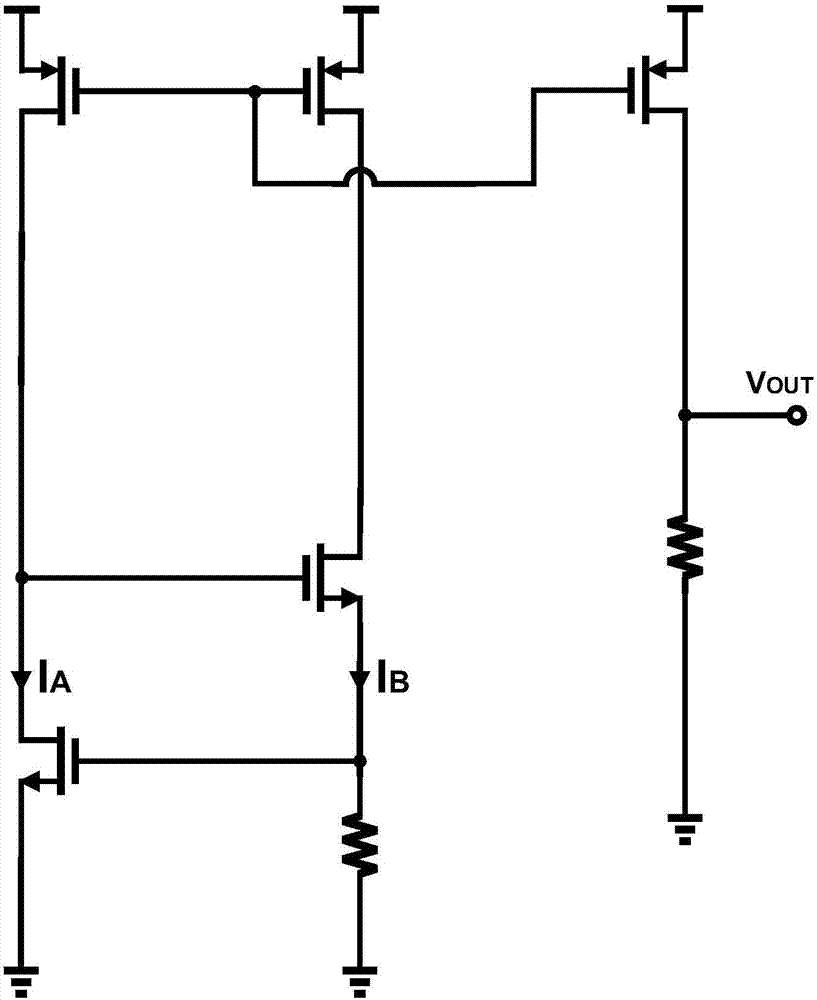
[0036] Such as Figure 5 shown, start-up circuit 2 is used to figure 2 The shown reference voltage source 3 based on the threshold voltage, the output voltage of the reference voltage source 3 based on the threshold voltage is V OUT , different from Embodiment 1, the first voltage control circuit 101 further includes a second diode D2 and a fourth NMOS transistor NMOS4. Wherein, the second diode D2 is connected in series between the power supply voltage and the first diode D1, the anode of the second diode D2 is connected to the power supply voltage, and the cathode of the second diode D2 is connected to the first diode positive terminal of tube D1. NMOS4 is connected in series between NMOS3 and NMOS2, the drain of NMOS4 is electrically connected to the source of NMOS3, the source of NMOS4 is electrically connected to the drain of NMOS2, and the gate of NMOS4 is electrically connected to the gate of NMOS3.

[0037] In this embodiment, the first voltage control circuit 101 ...


PUM


Abstract

The invention discloses a startup circuit for use in a reference voltage source. The startup circuit comprises a first NMOS (N-channel metal oxide semiconductor) transistor and a first PMOS (P-channel metal oxide semiconductor) transistor; a gate of the first NMOS transistor is connected with a first voltage control circuit that enables the first NMOS transistor to operate in a sub-threshold range, and a drain of the first NMOS transistor is electrically connected with a gate of the first PMOS transistor; the gate of the first PMOS transistor is connected with a second voltage control circuit, and current in the second voltage control circuit is proportional to current of the reference voltage source in magnitude; a source of the first PMOS transistor is connected with power supply voltage, a source of the first NMOS transistor is grounded, and a drain of the first PMOS transistor is used for providing output for the reference voltage source. The startup circuit provided herein has the advantage that since not a resistor but the first NMOS transistor is used, chip area used by the startup circuit is small and startup time is effectively improved.

Description

technical field [0001] The invention belongs to the technical field of integrated circuits, in particular to a starting circuit. Background technique [0002] Such as figure 1 The bandgap reference voltage source shown is used to generate a reference voltage V that is independent of temperature and supply voltage VDD BG , V BG The typical value of 1.2V (volts) or so. The traditional bandgap reference voltage source will fail when it starts up. At this time, I A = I B = 0, which causes V BG Also 0. figure 2 It is a reference voltage source based on the threshold voltage, and it also fails when it starts up. At this time, I A =I B = 0, which causes V OUT Also 0. In order to solve the above-mentioned problem of starting failure of the reference voltage source, a start-up circuit is usually added to the reference voltage source. The traditional start-up circuit contains several resistors. longer. Contents of the invention [0003] The technical problem to be solve...

Claims


Application Information

Patent Timeline
Patent Type & Authority Applications(China)
IPC IPC(8): G05F1/56
CPCG05F1/56
Inventor 李小勇李旋
Owner 上海韦玏微电子有限公司
Why Eureka
Try Eureka