Insulated gate bipolar transistor

A bipolar transistor and insulated gate technology, applied in semiconductor devices, electrical components, circuits, etc., can solve the problems of increasing turn-on energy consumption and large Miller capacitance, and achieve the effect of reducing Miller capacitance and turn-on energy consumption

Inactive Publication Date: 2017-12-01
CHANGZHOU ZHONGMING SEMICON TECH
View PDF4 Cites 8 Cited by
  • Summary
  • Abstract
  • Description
  • Claims
  • Application Information

AI Technical Summary

Problems solved by technology

[0004] figure 1 The disadvantage of the structure is that the Miller capacitance (Cres) between the gate and the collector is relatively large, which increases the turn-on energy consumption

Method used


Image

  • Insulated gate bipolar transistor
  • Insulated gate bipolar transistor
  • Insulated gate bipolar transistor

Examples


Embodiment 1

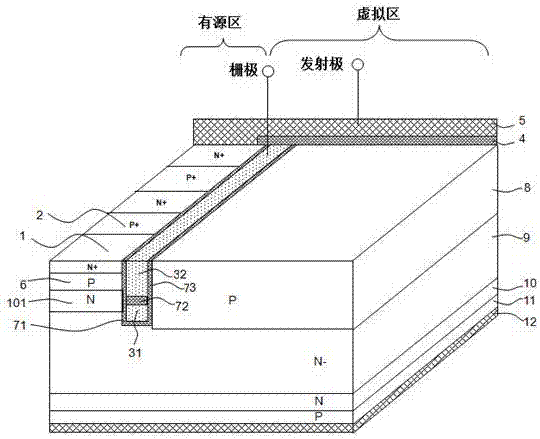
[0026] The structure of an insulated gate bipolar transistor of the present invention is as follows figure 2 As shown, including metal collector 12, P-type collector 11, N-type field stop layer 10 and N-drift region 9 on the back, the top of the transistor includes active original cell and dummy original cell, active original cell and dummy original cell Separated by trenches; the polysilicon filled in the trenches is separated into an upper polysilicon layer 32 and a lower polysilicon layer 31 by a dielectric layer 72, the upper polysilicon layer 32 and the oxide layer 73 on the upper part of the trench are in contact with each other, and the lower polysilicon layer 31 and the lower part of the trench are oxidized The layers 71 are in contact with each other; the upper polysilicon layer 32 is connected to the gate electrode, and the lower polysilicon layer 31 is connected to the emitter electrode; the active cell includes one or more N+ emitter regions 1 and a plurality of P+...

Embodiment 2

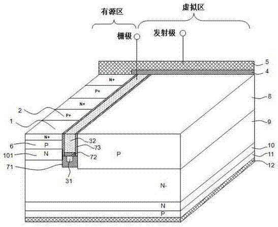
[0028] image 3 Shown is a modified structure of the present invention. Compared with the transistor structure of Embodiment 1, the thickness of the oxide layer 71 at the lower part of the trench is greater than the thickness of the oxide layer 73 at the upper part of the transistor in this embodiment. The advantage of this structure is that because the electric field at the bottom of the trench is relatively large, thickening the oxide layer at the bottom of the trench can enhance the reliability of the device.

[0029] The working principle of the present invention is as follows:

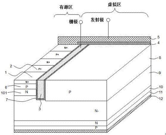
[0030] figure 1 In the structure shown, the polysilicon 3 inside the trench is connected to the gate electrode. The polysilicon 3 fills the entire trench, so the Miller capacitance caused by the polysilicon 3 is relatively large, which will adversely affect the performance of the device. For example, the voltage drop rate will be slower during the turn-on process, increasing the turn-on energy c...


PUM


Abstract

The invention discloses an insulated gate bipolar transistor. Compared with the prior art, polycrystalline silicon filled in a trench is separated by a dielectric layer into an upper polycrystalline silicon layer and a lower polycrystalline silicon layer, the upper polycrystalline silicon layer and the lower polycrystalline silicon layer are mutually contacted with an oxide layer at the upper part of the trench and an oxide layer at the lower part of the trench respectively, the upper polycrystalline silicon layer is connected with a gate electrode, and the lower polycrystalline silicon layer is connected with an emitting electrode; and bottom part of the upper polycrystalline silicon layer in the trench is deeper than a P-type well region of an active primitive cell. The structure disclosed by the invention reduces the Miller capacitance and the turn-on power consumption of the device.

Description

technical field [0001] The invention belongs to the technical field of power semiconductor devices, and in particular relates to an insulated gate bipolar transistor device (IGBT). Background technique [0002] IGBT not only can withstand high voltage and provide high current, but also is easy to control, and is an important device for high-power applications. There are various IGBT structural designs, among which the structure with dummy cells is more commonly used (see, for example, US Patent No. 8,633,510, hereinafter referred to as “Patent Document 1”). [0003] A typical IGBT structure described in Patent Document 1 is as figure 1 shown. The structure includes: a metal collector 12 on the back, a P-type collector 11 , an N-type field stop layer 10 and an N-drift region 9 . The top of the transistor includes an active primitive cell and a dummy primitive cell. Active and dummy cells are separated by trench gates. The trench gate structure is composed of polysilicon ...

Claims


Application Information

Patent Timeline
Patent Type & Authority Applications(China)
IPC IPC(8): H01L29/423H01L29/739
CPCH01L29/7398H01L29/42312H01L29/7397
Inventor 李宇柱
Owner CHANGZHOU ZHONGMING SEMICON TECH
Why Eureka
Try Eureka