Scattering device and manufacturing method thereof, light emitting device, projection system and lighting system
A light-emitting device and manufacturing method technology, applied in projection devices, optics, optical components, etc., can solve the problem of very high control requirements for the surface morphology of the scattering sheet, and achieve the effect of a small scattering angle
- Summary
- Abstract
- Description
- Claims
- Application Information
AI Technical Summary
Problems solved by technology
Method used
Image
Examples
Embodiment 1
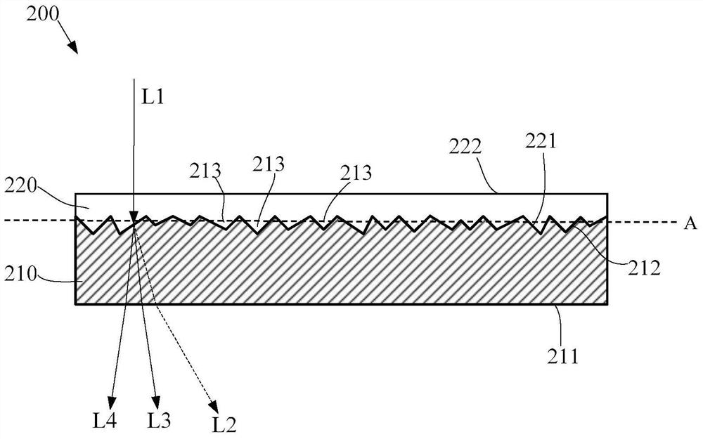
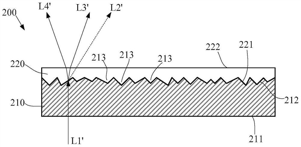
[0032] see Figure 2a and Figure 2b , Figure 2a and 2b is a schematic structural diagram of an embodiment of the scattering device in the embodiment of the present invention. like Figure 2a and 2b As shown, the scattering device 200 includes a transparent inorganic substrate 210 (shaded area) and a transition medium 220 (unshaded area).
[0033] The transparent inorganic substrate 210 includes a first surface 211 and a second surface 212 opposite to each other. Transparency in transparent inorganic substrates means that the substrate material is transparent and low-absorbing to the light to be scattered; there are many options for inorganic substances, such as silicon oxide (quartz), aluminum oxide, titanium oxide, etc., and may also be A mixture of various inorganic components, such as glass. The first surface is a plane, and the second surface 212 is a rough surface, and the rough surface has a plurality of micro depressions 213 . Generally speaking, whether chemi...
Embodiment 2
[0061] see image 3 , image 3 is a schematic structural diagram of another embodiment of the scattering device in the embodiment of the present invention. like image 3 As shown, the scattering device 300 includes a transparent inorganic substrate 310 (shaded area) and a transition medium 320 (unshaded area). The base 310 includes a first surface 311 and a second surface 312 opposite to each other, and the second surface 312 is a rough surface. The transition medium 320 covers the rough surface of the substrate 310 , and the transition medium 320 includes a third surface 321 and a fourth surface 322 opposite to each other.
[0062] The differences between this embodiment and the embodiment shown in Figure 2 include:
[0063] The fourth surface 322 of the transition medium is an arc surface, specifically a convex surface, and the convex surface is equivalent to a lens. The scattering device 300 can be regarded as two optical elements divided by the surface B, the upper su...
Embodiment 3
[0067] From the analysis in Embodiment 1, it can be seen that the transition medium does not necessarily have to fill the micro-depressions, but as long as there are micro-depressions filled, and the upper surface of the transition medium filled with micro-depressions is partially flat, the light L1 incident on this plane is The scattering angle can be reduced by the scattering device. Therefore, the present invention also provides another embodiment. see Figure 4a , Figure 4a is a schematic structural diagram of another embodiment of the scattering device in the embodiment of the present invention. like Figure 4a As shown, the scattering device 400 includes a transparent inorganic substrate 410 (shaded area) and a transition medium 420 (unshaded area).
[0068] The transparent inorganic substrate 410 includes a first surface 411 and a second surface 412 opposite to each other. The second surface 412 is a rough surface, and the rough surface has a plurality of micro dep...
PUM
 Abstract
Description
Claims
Application Information


