Split chip carrier board handling and bonding device
A bonding device, split-type technology, applied in the field of split-type chip carrier board handling bonding device, can solve the problems of long bonding time, low yield, difficulty in meeting mass production requirements, etc., to improve yield and save exposure the effect of time
- Summary
- Abstract
- Description
- Claims
- Application Information
AI Technical Summary
Problems solved by technology
Method used
Image

Examples
Embodiment Construction
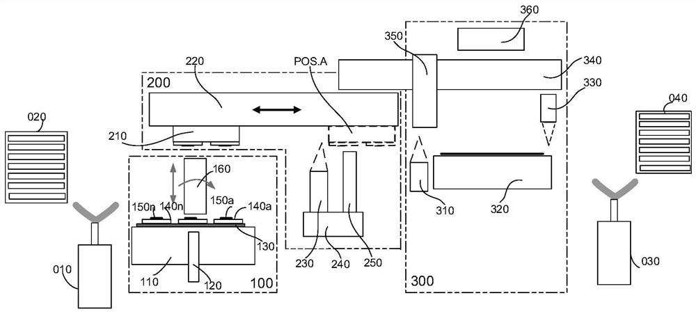
[0028] The following will combine Figure 1 to Figure 7 The split-type chip carrier handling and bonding device provided by the present invention is described in detail, which is an optional embodiment of the present invention, and it can be considered that those skilled in the art can make it Make revisions and polish.
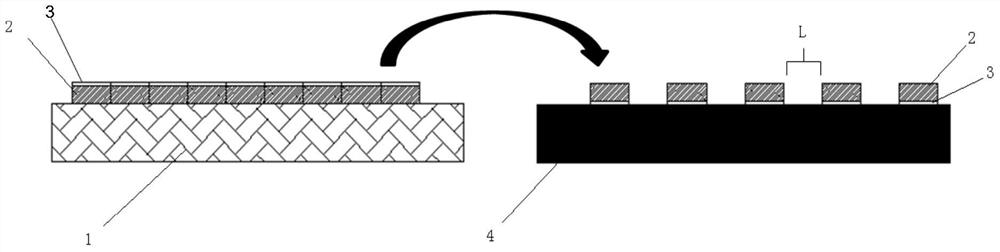
[0029] Please refer to figure 1 , which shows a schematic diagram of the flip-chip bonding process flow. The pre-bonded chip 2 is placed on the carrier 1 with the device surface 3 facing upward, and the bonded chip 2 is bonded to the substrate 4 by grabbing and flipping the robot. L The pitch for bonding chips can be adjusted according to different process requirements.
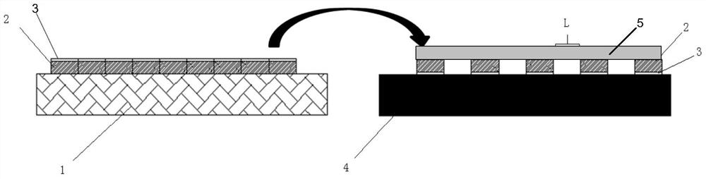
[0030] Please refer to figure 2 , where the plurality of chips 2 on the carrier 1 are batch-bonded to the substrate 4 in a manner carried by the carrier 5, and the plurality of chips 2 are accurately placed and adsorbed on the carrier 5, and the chips 2 are The space between the chip 2 ...
PUM
 Abstract
Description
Claims
Application Information
 - R&D
- Intellectual Property
- Life Sciences
- Materials
- Tech Scout
- Unparalleled Data Quality
- Higher Quality Content
- 60% Fewer Hallucinations
Browse by: Latest US Patents, China's latest patents, Technical Efficacy Thesaurus, Application Domain, Technology Topic, Popular Technical Reports.
© 2025 PatSnap. All rights reserved.Legal|Privacy policy|Modern Slavery Act Transparency Statement|Sitemap|About US| Contact US: help@patsnap.com