A test board for electrostatic discharge current waveform detection

A technology of current waveform and electrostatic discharge, which is applied in the field of test board structure and charged device model, can solve the problems of limited test range, inflexibility, and high cost, and achieve the effects of reducing production and maintenance costs, improving measurement quality, and solving the impact

Inactive Publication Date: 2017-12-12
SHANGHAI RES INST OF MICROELECTRONICS SHRIME PEKING UNIV
View PDF5 Cites 2 Cited by
  • Summary
  • Abstract
  • Description
  • Claims
  • Application Information

AI Technical Summary

Problems solved by technology

[0007] 2. During the test, the whole process cannot be carried out in an ideal environment
Since the test signal is a high-frequency signal, any bad contact or inappropriate position of the equipment will have a great impact on the test results
[0009] 4. The supporting equipment of the CDM test system currently used is mass-produced, and the cost is high, so it is not suitable for a small number of tests in small companies or laboratories
[0011] 1. High cost
In the actual environment, interference may come from various places. To achieve no interference, all-round protection must be achieved. All parts from the interference source to the transmission path must be protected. This n

Method used


Image

  • A test board for electrostatic discharge current waveform detection
  • A test board for electrostatic discharge current waveform detection

Examples


Embodiment

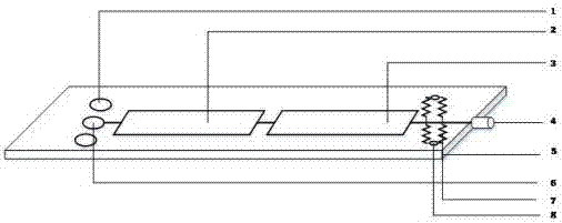
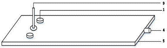
[0035] In an embodiment, the current discharge waveform of the CDM model detects a double-sided test board structure.

[0036] figure 1 and figure 2They are the top view and the bottom view of the double-sided test board structure in the first embodiment of the present invention respectively. It can be seen from the figure that the double-sided test board structure of this embodiment includes: a through-hole structure 1 with a fixing function on the back, which is used for installing screws or other fixtures; filter 2 for filtering out high-frequency interference; attenuator 3 for reducing current peaks to facilitate testing; grounding plate grounding metal socket 4, used to connect the oscilloscope and the test board through a coaxial cable; The ground plate 5 that connects all parts, collects each module and has a grounding effect, and can be connected with other parts of the test system; pogo (pogo stick) probe 6, the part on the back of the test board is the probe base, ...


PUM


Abstract

The invention provides a test board structure for CDM (Charged Device Model) ESD current waveform detection, which is used for effectively catching discharge current waveforms consistent with typical waveforms in international general test standards. The test board comprises a pogo probe used for direct contact with a discharge device, a filter used for filtering away high frequency interference, an attenuator used for reducing current peak values and facilitating testing, a testing resistor used for converting current signals and an earth plate used for connecting all the parts. The filter and the attenuator are located on the earth plate; the earth plate is connected with a metal socket to be connected with an oscilloscope; the earth plate comprises a structure for fixing, which is used for connection with other parts of a testing system.

Description

technical field [0001] The invention relates to the field of integrated circuits, in particular to a test board structure for detecting a charged device model (CDM, Charged Device Model) electrostatic discharge current waveform in an electrostatic discharge (ESD, Electro-Static discharge) test. Background technique [0002] With the development of technology, integrated circuit components tend to be more and more miniaturized and complicated. Usually, the number of transistors and other semiconductor devices contained in a small device reaches millions. Due to the extremely high density of transistors in the device, a small damage can lead to the scrapping of the entire device. Among the various electrostatic damages that devices may encounter, the CDM model is particularly noteworthy, not only because of its fast discharge speed, which often makes the protection circuit too late to conduct and cannot play a protective role, but also because the current detection of the ESD ...

Claims


Application Information

Patent Timeline
IPC IPC(8): G01R19/00G01R19/04
CPCG01R19/0061G01R19/04
Inventor 陆宇陈昭程玉华
Owner SHANGHAI RES INST OF MICROELECTRONICS SHRIME PEKING UNIV
Why Eureka
Try Eureka