Superjunction power device

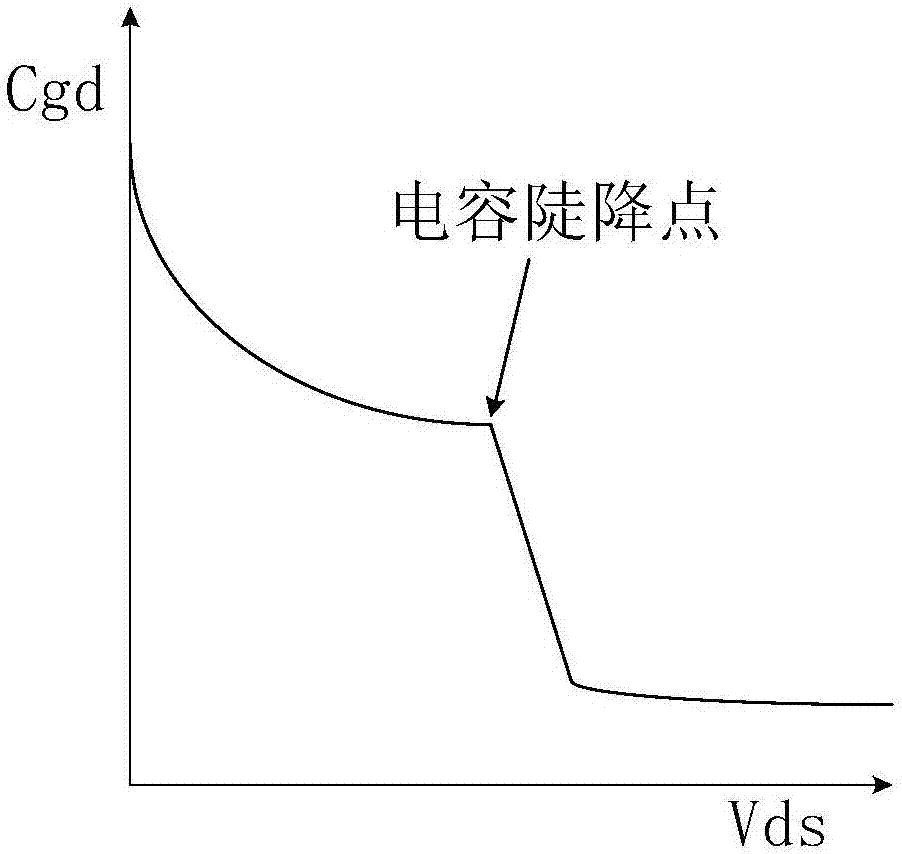
A technology of power devices and gate structures, applied in semiconductor devices, electrical components, circuits, etc., can solve problems such as Cgd slow change, and achieve the effect of alleviating sudden changes and reducing oscillations

Active Publication Date: 2017-12-12
UNIV OF ELECTRONICS SCI & TECH OF CHINA
View PDF6 Cites 6 Cited by
  • Summary
  • Abstract
  • Description
  • Claims
  • Application Information

AI Technical Summary

Problems solved by technology

However, the sharp drop of Cgd in superjunction devices is mainly caused by the mutual depletion of PN columns rather than the depletion of JFET regions between adjacent body regions. To the effect of making Cgd gradually change

Method used


Image

  • Superjunction power device
  • Superjunction power device
  • Superjunction power device

Examples


Embodiment 1

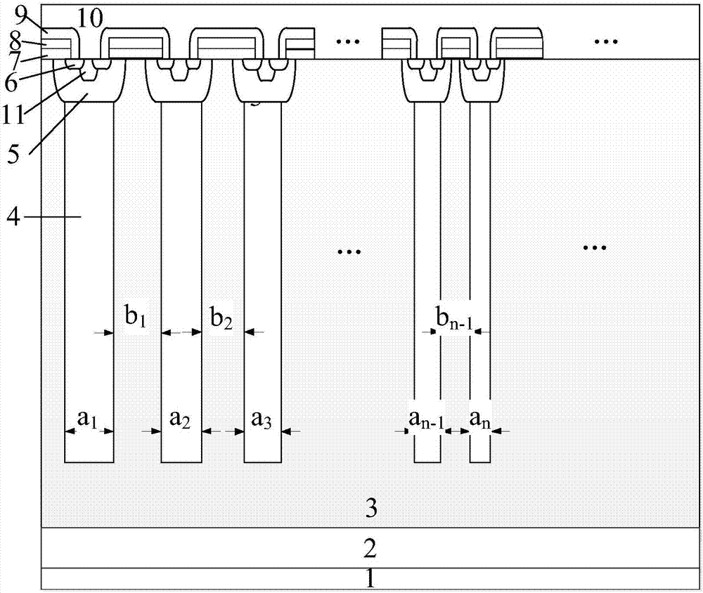
[0014] A super junction power device such as figure 2 As shown, it includes a metallized drain 1, a heavily doped substrate 2 of the first conductivity type, a lightly doped epitaxial layer 3 of the first conductivity type and a metallized source 10 stacked sequentially from bottom to top; There is a semiconductor column 4 of the second conductivity type in the lightly doped epitaxial layer 3; there is a semiconductor body region 5 of the second conductivity type between the semiconductor column 4 of the second conductivity type and the lower surface of the metallized source electrode 11, and the semiconductor body region 5 of the second conductivity type The upper layer of the second conductivity type semiconductor body region 5 has the first conductivity type semiconductor source region 6 and the second conductivity type semiconductor heavily doped contact region 11 which are independent and contacting each other, and the second conductivity type semiconductor heavily doped ...

Embodiment 2

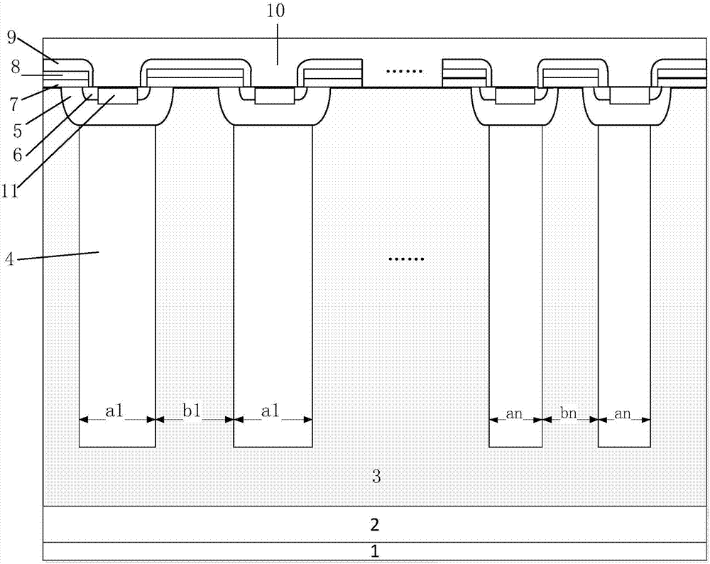
[0029] A super junction power device such as image 3 As shown, the metallized drain 1, the first conductivity type semiconductor substrate 2, the first conductivity type lightly doped epitaxial layer 3 and the metallized source 10 are stacked in sequence from bottom to top; the first conductivity type lightly doped The epitaxial layer 3 has a second conductivity type semiconductor column 4; the top of the second conductivity type semiconductor column 4 has a second conductivity type semiconductor body region 5; the second conductivity type semiconductor body region 5 has a first conductivity type The semiconductor source region 6 and the second conductivity type semiconductor heavily doped contact region 11, the second conductivity type semiconductor body region 5 between the first conductivity type semiconductor 6 and the adjacent first conductivity type lightly doped epitaxial layer 3 It is a channel region; a gate oxide layer 7 covers the channel region and the lightly dop...


PUM


Abstract

The invention relates to the technical field of a power semiconductor device, in particular to a superjunction power device. In the superjunction power device provided by the invention, each second conductive type of semiconductor post in a first conductive type of semiconductor drift region has two or more than two different widths (a1, a2 until an, and n is more than or equal to 2), and the distance between two adjacent second conductive types of semiconductor posts has two or more than two different widths (b1, b2 until bm, and m is more than or equal to 2). The corresponding drain-source voltage points which are consumed by the superjunction post and have different widths and distances are different, thus, abruptly-reduced source-drain voltage span of a miller capacitor Cgd and a source-drain capacitor Cds is increased, abrupt reduction of the Cgd and the Coss is relieved, and the current-voltage oscillation is reduced.

Description

technical field [0001] The invention relates to the technical field of power semiconductor devices, in particular to a super junction power device. Background technique [0002] Capacitance characteristics are crucial to the turn-on and turn-off processes of power DMOS devices, which will affect the switching speed and EMI (Electromagnetic Interference) characteristics of the device. Due to the difference in the structure of the drift region of the super-junction VDMOS and the conventional VDMOS, its capacitance characteristics are also different: the output capacitance (Coss) and Miller capacitance (Cgd) curves of the super-junction VDMOS will show a high degree of non-linearity with the increase of the drain-source voltage. linear relationship. Because of the high cell density, the initial value of Coss of super-junction VDMOS is high, and Coss and Cgd will drop sharply near a specific drain-source voltage, such as figure 1 As shown, the reason is that the N column is co...

Claims


Application Information

Patent Timeline
Patent Type & Authority Applications(China)
IPC IPC(8): H01L29/06H01L29/78
CPCH01L29/0634H01L29/7802
Inventor 任敏李佳驹苏志恒李泽宏高巍张金平张波
Owner UNIV OF ELECTRONICS SCI & TECH OF CHINA
Why Eureka
Try Eureka