BPS array substrate and making method thereof

A technology of an array substrate and a manufacturing method, which are applied in the field of BPS type array substrate and its manufacture, can solve the problems of poor film thickness uniformity, incomplete cross-linking reaction, insufficient UV light dose, etc., so as to achieve low production cost and improve product competitiveness. , easy-to-control effects

Inactive Publication Date: 2017-12-22
SHENZHEN CHINA STAR OPTOELECTRONICS SEMICON DISPLAY TECH CO LTD
View PDF5 Cites 11 Cited by
  • Summary
  • Abstract
  • Description
  • Claims
  • Application Information

AI Technical Summary

Problems solved by technology

[0008] In the existing BPS technology, the area corresponding to the Main PS (Tr3 = 100%) has received a sufficient dose of UV light, and the crosslinking reaction is relatively complete, so the film thickness will basically not change; while the area corresponding to the Sub PS and BM ( Tr2=0%~100%) Due to insufficient UV light dose and incomplete cross-linking reaction, it is easily affected by various factors in the development environment during the development process, resulting in poor film thickness uniformity of Sub PS and BM

Method used


Image

  • BPS array substrate and making method thereof
  • BPS array substrate and making method thereof
  • BPS array substrate and making method thereof

Examples


Embodiment Construction

[0044] In order to further illustrate the technical means adopted by the present invention and its effects, the following describes in detail in conjunction with preferred embodiments of the present invention and accompanying drawings.
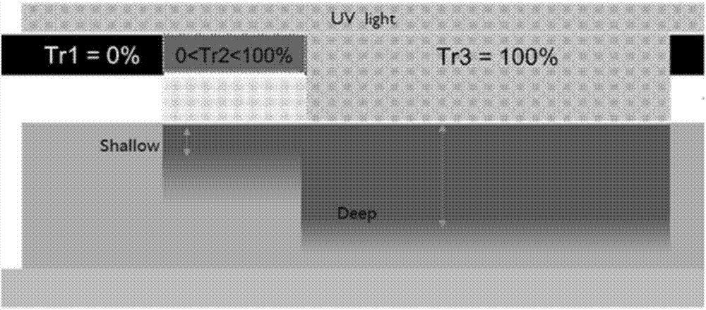
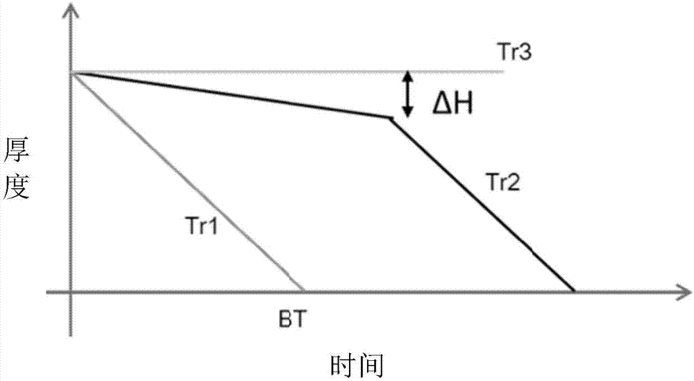
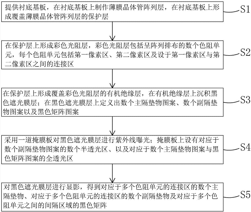
[0045] The idea of ​​the present invention is to combine BPS technology with COA (Color Filter on Array) technology, not only make black matrix 83, main spacer 81, and auxiliary spacer 82 on the array substrate, but also color light The resist layer 40 is fabricated on the array substrate, and the height difference between the main spacer 81 and the black matrix 83 is realized by using the height of the color resist unit 41 , and the light transmittance of the mask plate 70 is controlled by using the thickness of the color resist unit 41 To realize the height difference between the sub spacers 82 and the black matrix 83 .

[0046] see image 3 , the present invention provides a method for manufacturing a BPS type array substrate, comprising t...


PUM

PropertyMeasurementUnit
transmittivityaaaaaaaaaa

Abstract

The invention provides a BPS array substrate and a making method thereof. The making method includes that a black matrix, a main spacer and an auxiliary spacer are arranged on the array substrate and realized in a same making process, so that production time can be reduced, production cost is lowered, and product competitiveness is improved; height difference of the main spacer and the black matrix is realized by utilizing thickness of a color resistance unit, height difference of the auxiliary spacer and the black matrix is realized by utilizing the thickness of the color resistance unit and controlling light transmittance of a mask, so that height of the main spacer and the auxiliary spacer is easier to control; a mask area corresponding to an area, correspondingly forming the black matrix, of a black light shielding coating during exposure is a full light-pervious area, ultraviolet irradiation received during exposure is sufficient, and crosslinking reaction is complete, so that stability is high; influence of developing liquid is small in the process of developing, the black matrix cannot be dissolved, so that coating thickness uniformity of the black matrix is ensured to be high.

Description

technical field [0001] The present invention relates to the field of display technology, in particular to a BPS type array substrate and a manufacturing method thereof. Background technique [0002] With the development of display technology, liquid crystal displays (Liquid Crystal Display, LCD) and other flat display devices have become the mainstream of display devices and are widely used due to their advantages of high image quality, power saving, thin body and wide application range. Used in mobile phones, TVs, personal digital assistants, digital cameras, notebook computers, desktop computers and other consumer electronics products. [0003] Most of the liquid crystal display devices currently on the market are backlight liquid crystal display devices, which include a backlight module, a liquid crystal panel combined with the backlight module, and a front frame for fixing the liquid crystal panel and the backlight module. The working principle of the liquid crystal pan...

Claims


Application Information

Patent Timeline
Patent Type & Authority Applications(China)
IPC IPC(8): G02F1/1339G02F1/1362G02F1/1368G02F1/1335
CPCG02F1/133512G02F1/133514G02F1/13394G02F1/136209G02F1/1368G02F1/136295G02F1/13398G02F1/13396G02F1/136222G02F1/13392
Inventor 于承忠
Owner SHENZHEN CHINA STAR OPTOELECTRONICS SEMICON DISPLAY TECH CO LTD
Why Eureka
Try Eureka