Epitaxial film deposition system and epitaxial film formation method

Inactive Publication Date: 2006-11-09
FUJI ELECTRIC HLDG CO LTD
View PDF6 Cites 17 Cited by
  • Summary
  • Abstract
  • Description
  • Claims
  • Application Information

AI Technical Summary

Benefits of technology

[0017] By supplying the reactant gas from both the ends of the tubular reactor (as opposed to flowing the reactant gas along one direction within the reactor), the epitaxial film which is formed on the wafer has good uniformity of film quality and film thickness and the like, while this epitaxial film deposition system does not require any wafer rotation mechanism. Accordingly, it becomes possible to perform formation of an epitaxial film on the wafer which is kept stationary, with the reactant gas being supplied alternately from mutually different directions over the surface of the wafer on which the epitaxial film is to be formed, the directions being approximately parallel to the surface of the wafer.
[0018] With the

Problems solved by technology

However, when forming an SiC film by epitaxial growth during the formation of a semiconductor device, the current situation is that there is no effective unit which can reliably prevent crystal defects such as so-called micro pipes and stacking faults, such as are sometimes created during such film formation.
However, there has been the problem that, when forming an SiC epitaxial film with such a prior art epitaxial film deposition system, it is not possible to satisfy, simultaneously and at a high level, the full width and so on of the range of process conditions, not only such as crystalline product quality, film thickness uniformity, and impurity density uniformity, but also temperature and pressure and the like.
This is because the reactant gas progressively crystallizes on the wafer in order from upstream, so that the composition of the reactant gas progressively changes as it passes downstream, which is undesirable, and it is a problem which theoretically cannot be avoided.
However since, for epitaxial growth of SiC, its growing temperature is 1500° C. even-when low, and exceeds 2000° C. when high, accordingly there have been difficult problems with providing such a wafer rotation mechanism within the epitaxial film deposition system, with regard to its own structure.
On the other hand, when the rotation shaft which is connected to the susceptor is made from graphite just as is the susceptor itself, due to heat conduction, he

Method used


Image

  • Epitaxial film deposition system and epitaxial film formation method
  • Epitaxial film deposition system and epitaxial film formation method
  • Epitaxial film deposition system and epitaxial film formation method

Examples


first embodiment

[0030] First, the invention will be explained.

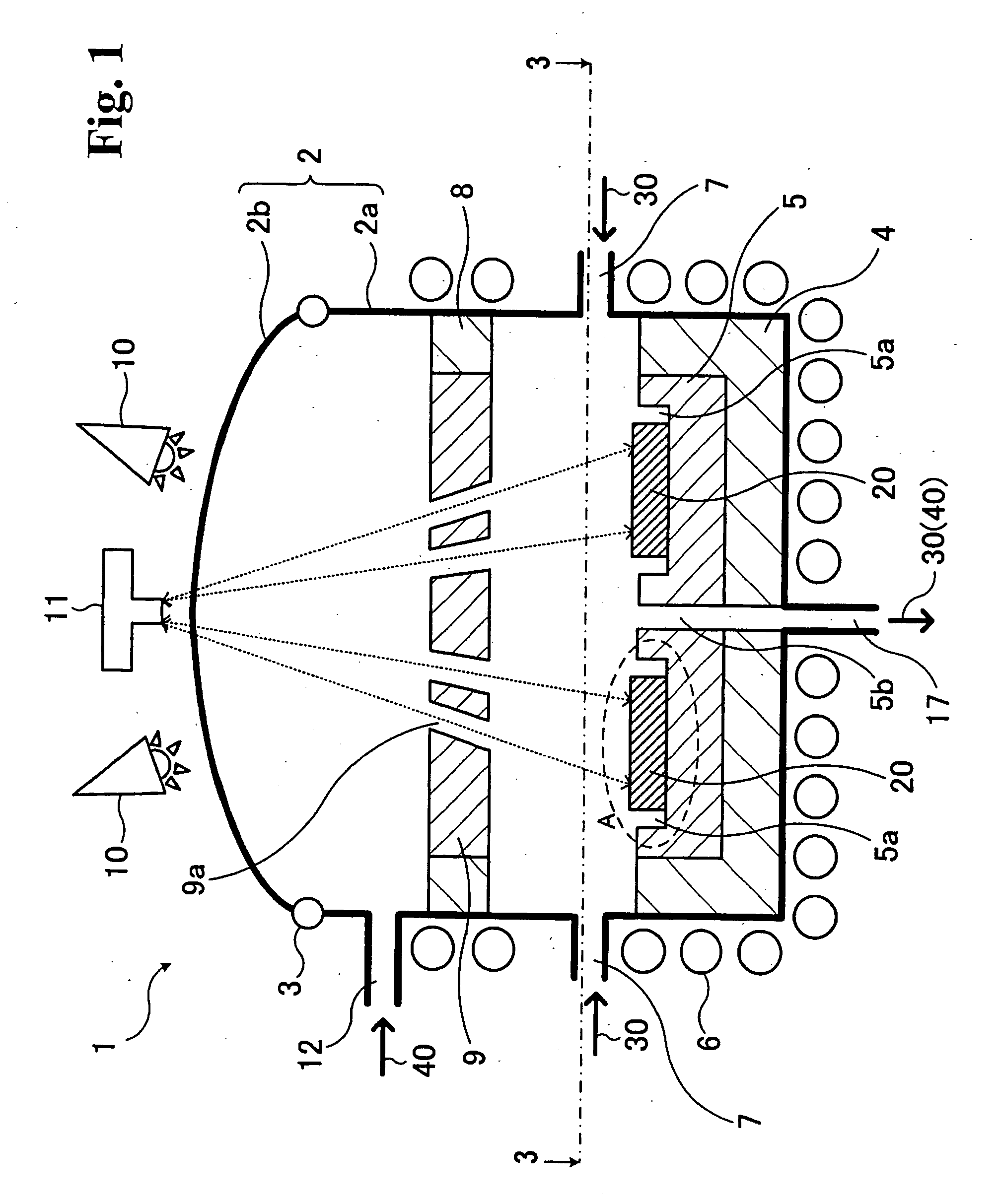
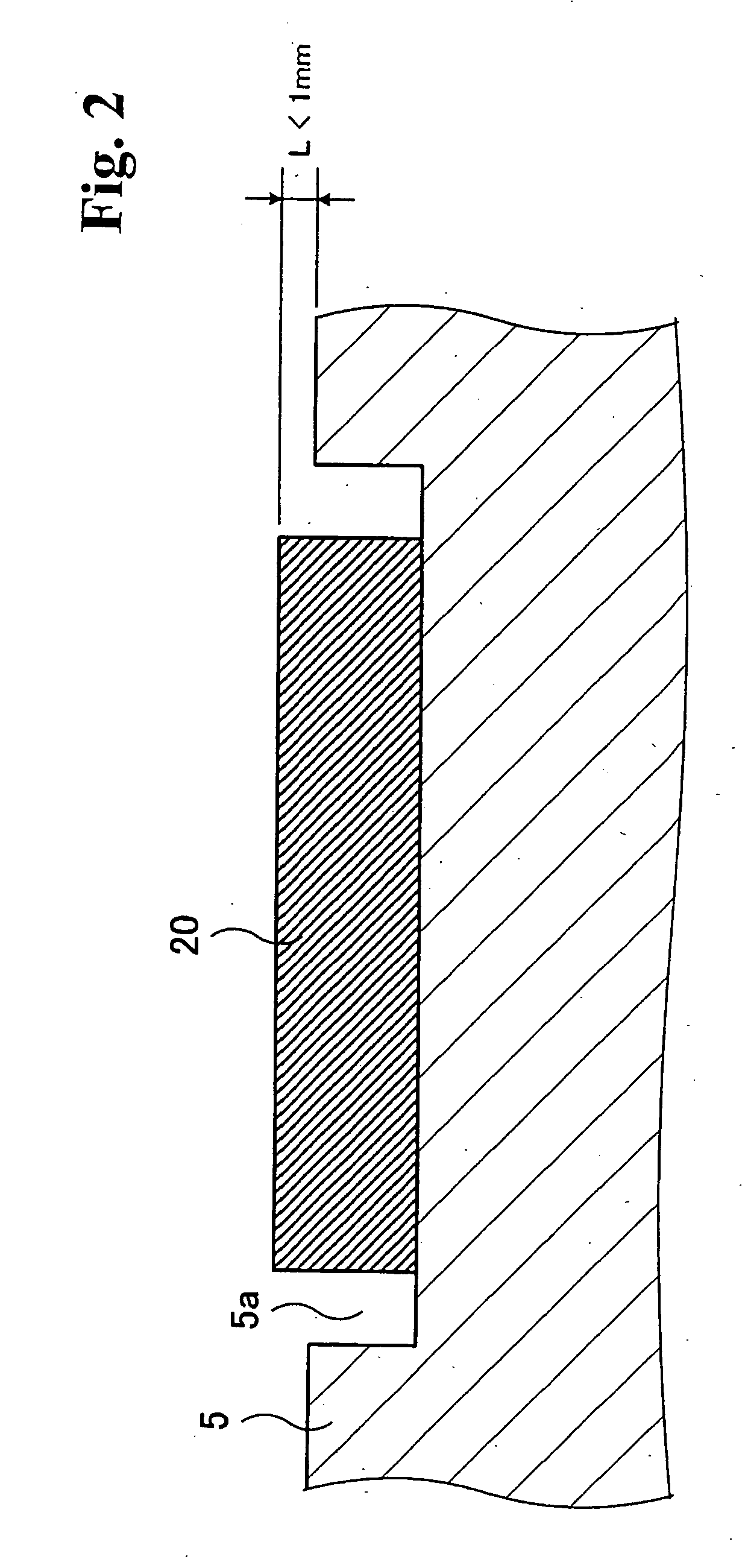
[0031]FIG. 1 is a schematic cross-sectional view showing the main portions of an epitaxial film deposition system according to the first embodiment; FIG. 2 is an enlarged view of a portion A of FIG. 1; FIG. 3 is a schematic cross-sectional view of this epitaxial film deposition system according to the first embodiment taken looking in a direction shown by the arrows 3-3 in FIG. 1; and FIG. 4 is a schematic plan view of the main portions of the epitaxial film deposition system according to the first embodiment. The epitaxial film deposition system 1 shown in FIG. 1 comprises a reactor 2 which comprises a reaction vessel 2a made from quartz glass and a lid 2b also made from quartz glass; the lid 2b is fitted on the reaction vessel 2a via an O-ring 3, so that the interior of the reactor 2 is tightly sealed. In its overall shape, this reactor 2 is made with its side portion shaped as a cylindrical tubular interior wall, and with its upper po...

second embodiment

[0068] Next, the present invention will be explained.

[0069]FIG. 5 is a schematic cross-sectional figure showing the main portions of an epitaxial film deposition system according to the second embodiment of the present invention, and FIG. 6 is a schematic cross-sectional figure of this epitaxial film deposition system according to the second embodiment, taken looking in a direction shown by the arrows 6-6 in FIG. 5. In FIGS. 5 and 6, to structural elements which are the same as ones appearing in FIGS. 1 and 3, the same reference symbols will be appended, and the explanation thereof will be omitted.

[0070] The epitaxial film deposition system 50 shown in FIGS. 5 and 6 differs from the epitaxial film deposition system 1 of the first preferred embodiment described above which was made so as to perform batch processing on a plurality of the SiC wafers 20, by the feature that the epitaxial film deposition system 50 performs processing of one SiC wafer 20 at a time.

[0071] With this epita...

third embodiment

[0076] Next, the present invention will be explained.

[0077]FIG. 7 is a schematic cross-sectional figure showing the main portions of an epitaxial film deposition system according to this third embodiment of the present invention. To structural elements which are the same as ones appearing in FIG. 1, the same reference symbols will be appended, and the explanation thereof will be omitted.

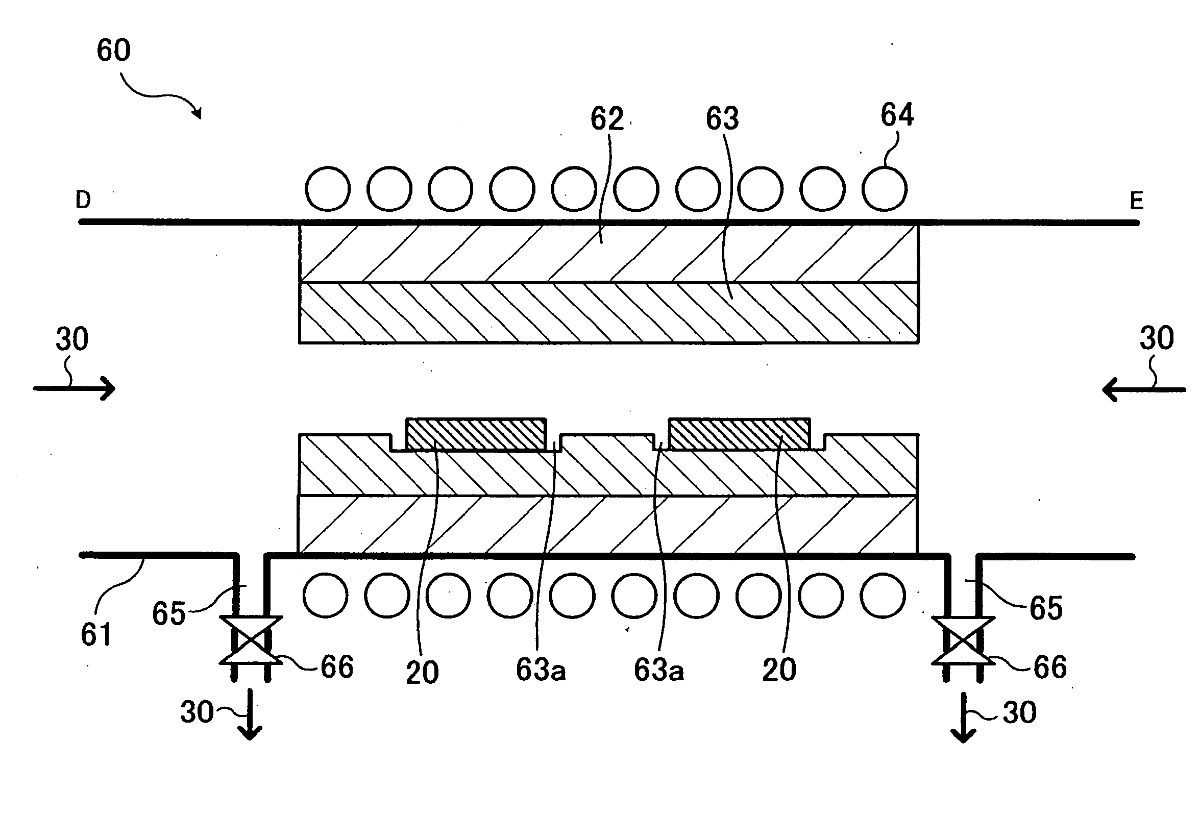
[0078] The epitaxial film deposition system 60 shown in FIG. 7 comprises a reactor 61 which is made from quartz, and an insulation 62 is disposed circumferentially around a predetermined region of its interior wall, with a susceptor 63 being further disposed circumferentially -on the inside of this insulation 62. Two countersinks 63a are formed in a portion of the susceptor 63, and it is arranged to mount one SiC wafer 20 in each of these. It should be understood that the step between the susceptor 63 and the SiC wafers 20 are kept within a predetermined range, so as not to cause any turbulence in t...


PUM


Abstract

An epitaxial film deposition system includes a reactor, a susceptor, a wafer heating unit, a reactant gas supply orifice, and an aperture for venting the reactant gas. The reactant gas is supplied to a reactor region between the susceptor and a graphite plate so as to circulate in layered flow in a direction along the reactor inner wall in the planar direction of a mounted SiC wafer. The temperature of the wafer is controlled by a high frequency coil and halogen lamps based on temperatures detected by a pyrometer. By circulating the reactant gas over the surface of the stationary wafer, it is possible to form, under various process conditions, an SiC epitaxial film having good film quality and good uniformity of film thickness, without providing any wafer rotation mechanism.

Description

BACKGROUND OF THE INVENTION AND RELATED ART STATEMENT [0001] The present invention relates to an epitaxial film deposition system and an epitaxial film deposition method, and in particular, relates to an epitaxial film deposition system and an epitaxial film deposition method which are used in formation of an epitaxial film of silicon carbide (SiC) or silicon (Si) or the like. [0002] Although Si is the main material used at the moment for semiconductor devices, it is predicted that the replacement thereof by SiC will progress from now onward, in particular in the field of semiconductor devices for electric power or the like. However, when forming an SiC film by epitaxial growth during the formation of a semiconductor device, the current situation is that there is no effective unit which can reliably prevent crystal defects such as so-called micro pipes and stacking faults, such as are sometimes created during such film formation. It is strongly desirable to provide a stable unit for...

Claims


Application Information

Patent Timeline
IPC IPC(8): H01L21/44H01L21/76
CPCC30B25/12C30B25/14H01L21/0262H01L21/02529H01L21/02378
Inventor KISHIMOTO, DAISUKETAWARA, TAKESHIIZUMI, SHUNSUKE
Owner FUJI ELECTRIC HLDG CO LTD
Why Eureka
Try Eureka