Method for manufacturing soi wafer

a technology of soi wafer and film thickness, which is applied in the direction of semiconductor/solid-state device manufacturing, basic electric elements, electric apparatus, etc., can solve the problems of deterioration of the film thickness uniformity of the soi layer achieved by implantation and delamination of hydrogen ions and others, and the surface roughness is considerable, so as to improve the yield of the device and improve the film thickness uniformity

Active Publication Date: 2014-11-06
SHIN-ETSU HANDOTAI CO LTD
View PDF4 Cites 19 Cited by
  • Summary
  • Abstract
  • Description
  • Claims
  • Application Information

AI Technical Summary

Benefits of technology

[0043]As described above, according to the method for manufacturing an SOI wafer of the present invention, the thermal oxide film having the substantially concentric film thickness distribution can be formed in the thermal oxidation of the sacrificial oxidation treatment. Therefore, since the SOI wafer having the dramatically improved film thickness uniformity can be eventually manufactured in the mass-volume production level, a threshold voltage of a device using such an SOI wafer can be stabilized, thereby improving a device yield.

Problems solved by technology

However, in case of fabricating an SOI wafer based on the ion implantation delamination method, a damage layer formed due to the ion implantation is present on a surface of the SOI wafer after the delamination, and surface roughness is considerable as compared with a mirror surface of a regular product level silicon wafer.
However, when polishing including a machining element is performed with respect to the SOI layer, since the stock removal of the polishing is not uniform, there occurs a problem that film thickness uniformity of the SOI layer achieved by implantation and delamination of hydrogen ions and others is deteriorated.

Method used


Image

  • Method for manufacturing soi wafer
  • Method for manufacturing soi wafer
  • Method for manufacturing soi wafer

Examples


example 1

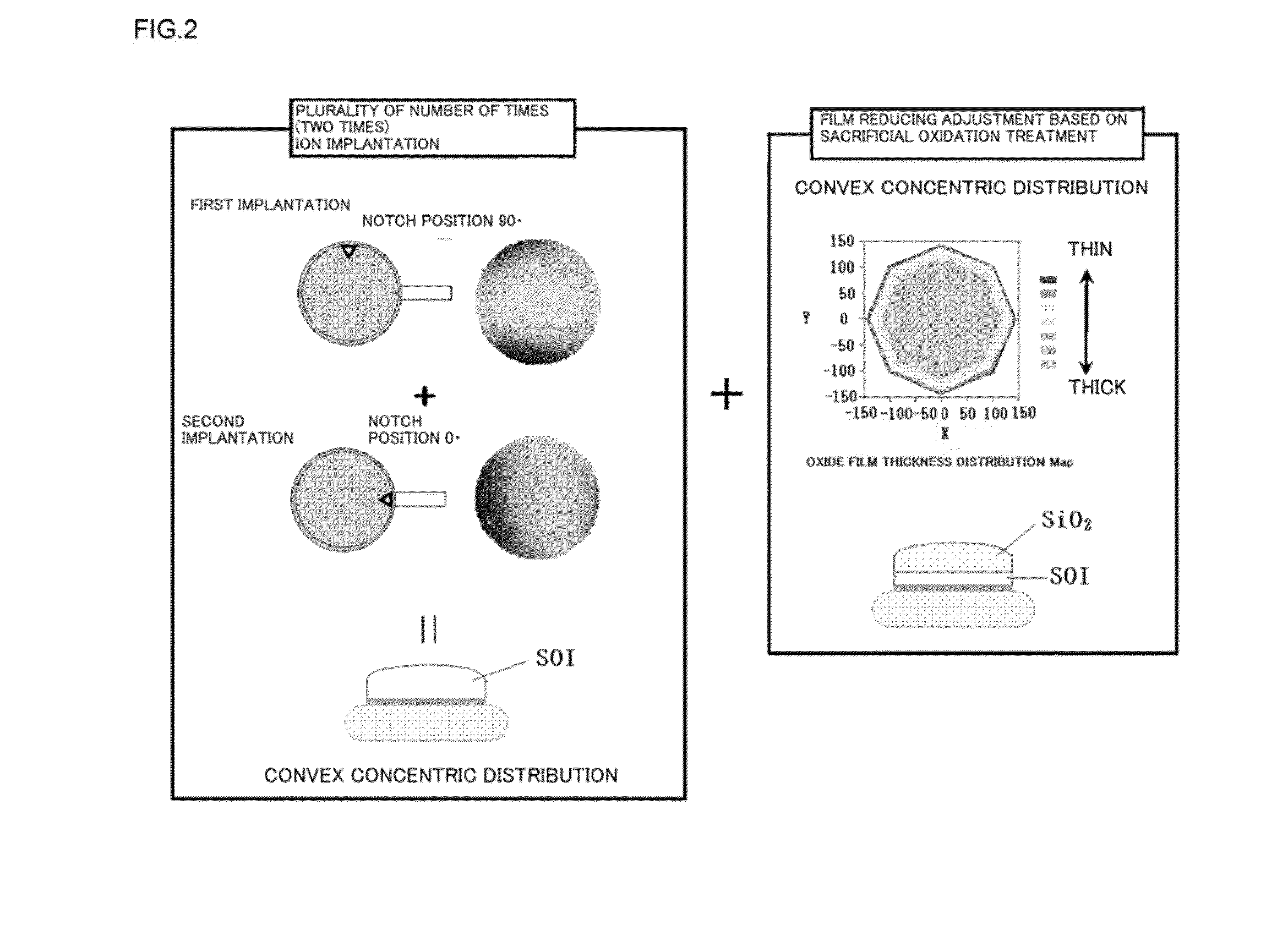
[0082]In Example 1, a buried oxide film that is 25 nm thick was fabricated on a silicon wafer with a diameter of 300 mm made of silicon single crystal having a crystal orientation (a crystal plane on a surface is precisely (100) without an angular deviation), and then hydrogen ion implantation was carried out. The ion implantation was divisionally carried out in two steps with the use of a batch processing ion implanter, first implantation was performed with H+, 30 keV, 2.6 e16 cm−2, an implantation angle of 0 degree, and a notch orientation angle of 0 degree, and second implantation was effected with H+, 30 keV, 2.6e16 cm−2, an implantation angle of 0 degree, and a notch orientation angle of 90 degrees. After the hydrogen ion implantation, the wafer was bonded to a base wafer and delaminated at a hydrogen ion implanted layer by a nitrogen atmosphere heat treatment performed at 500° C. for 30 minutes. Thereafter, as shown in FIG. 3, a temperature-fall oxidation treatment for contin...

example 2

[0084]After the ion implantation delamination was performed like Example 1, as shown in FIG. 3, the conventional oxidation at a fixed temperature of 900° C. was effected (the thermal oxidation (1)). An oxide film thickness after the thermal oxidation was 250 nm. A concentric distribution was out of shape, and a radial oxide film thickness Range of 0.4 nm. Then, the flattening heat treatment was performed in an Ar atmosphere, the temperature-fall oxidation treatment for continuing the pyrogenic oxidation treatment until 900° C. was carried out during the falling of a temperature after the pyrogenic oxidation treatment effected at 950° C. (the thermal oxidation (2)). A oxide film thickness after the thermal oxidation was 440 nm. A oxide film thickness distribution was measured by using a PW monitor, a radial oxide film thickness Range (Max−Min) provided by the temperature-fall oxidation treatment was 1.4 nm, and a concentric distribution that is thick at a central portion and thin at ...

example 3

[0086]A thin film SOI wafer having an SOI film thickness of 10 nm was fabricated under the same conditions as those of Example 1 except that the thermal oxidation (2) of Example 1 is the temperature-fall oxidation that is the same as the thermal oxidation (2) in Example 2. In regard to a film thickness distribution of a 10-nm SOI, Range was 0.5 nm, and the very excellent radial distribution was obtained.


PUM

PropertyMeasurementUnit
rotation anglesaaaaaaaaaa

Abstract

A method for manufacturing a SOI wafer, including a step of performing a thickness reducing adjustment to a SOI layer of the SOI wafer by carrying out a sacrificial oxidation to the SOI wafer for effecting thermal oxidation to a surface of the SOI layer and removing a formed thermal oxide film, wherein, when the thermal oxidation in the sacrificial oxidation treatment is carried out with the use of a batch processing heat treatment furnace during the rising of a temperature and / or the falling of a temperature, a substantially concentric oxide film thickness distribution is formed on the surface of the SOI layer. The result is a method for manufacturing a SOI wafer that enables manufacturing a SOI wafer that has improved radial film thickness distribution with good productivity by performing the sacrificial oxidation treatment for forming a substantially concentric oxide film and removing the formed thermal oxide film.

Description

TECHNICAL FIELD[0001]The present invention relates to a method for manufacturing an SOI wafer, and more particularly to a method for manufacturing an SOI wafer by boning a silicon single crystal wafer having hydrogen ions implanted therein to a base wafer that serves as a support substrate through an oxide film and then delaminating the silicon single crystal wafer.BACKGROUND ART[0002]In recent years, as a method for manufacturing an SOI wafer, a method for manufacturing an SOI wafer by bonding an ion-implanted bond wafer and then delaminating the same (an ion implantation delamination method: a technology that is also called a smart cut method (a registered trademark)) has newly begun to attract attention. This ion implantation delamination method is a technology for, e.g., forming an oxide film (an insulator film) on at least one of two wafers, implanting gas ions such as hydrogen ions or rare gas ions from an upper surface of one silicon wafer (a bond wafer), forming a micro bubb...

Claims


Application Information

Patent Timeline
Patent Type & Authority Applications(United States)
IPC IPC(8): H01L21/762H01L21/02H01L21/3105
CPCH01L21/76254H01L21/02318H01L21/02112H01L21/3105H01L21/26506H01L21/2658H01L21/68764H01L21/68771
Inventor AGA, HIROJIKOBAYASHI, NORIHIRO
Owner SHIN-ETSU HANDOTAI CO LTD
Why Eureka
Try Eureka