Method for manufacturing resist pattern and method for manufacturing semiconductor device

a technology of resist pattern and manufacturing method, which is applied in the direction of photosensitive material processing, photomechanical equipment, instruments, etc., can solve the problems of pattern defect and more serious problems, and achieve the effect of improving material efficiency, easy formation, and excellent uniform film thickness

Inactive Publication Date: 2008-07-29
SEMICON ENERGY LAB CO LTD
View PDF28 Cites 18 Cited by
  • Summary
  • Abstract
  • Description
  • Claims
  • Application Information

AI Technical Summary

Benefits of technology

[0014]The present invention of using ink jetting has an advantage of being excellent at uniformity of a film thickness and the like compared with a screen printing method in which the thin film (typically, a light-emitting layer) is formed by applying a solution, using a printing roll or a relief printing in which a pattern to be printed is printed, and then baking.
[0015]According to the present invention having the above-described structure, the resist pattern can be easily formed over the large sized substrate having a side of over one meter on a side. Since a step of the spin coating is not required in the present invention and a smaller amount of the wasted material is left, the efficiency in the use of a material can be enhanced and the manufacturing cost can be reduced.
[0016]According to the present invention in which the resist pattern is formed under reduced pressure, generation of dust added to the resist pattern and reforming of a surface in which the surface of the object to be processed is oxidized can be prevented.

Problems solved by technology

These problems become more serious when the coating film of the resist is formed over a large sized substrate.
Then, a resist at the edge portion is scraped in handling of the substrate, the scraped resist attaches to the substrate, and consequently a pattern defect is caused.

Method used


Image

  • Method for manufacturing resist pattern and method for manufacturing semiconductor device
  • Method for manufacturing resist pattern and method for manufacturing semiconductor device
  • Method for manufacturing resist pattern and method for manufacturing semiconductor device

Examples


embodiment mode 1

[0033]Embodiment mode of the present invention is described in detail with reference to drawings. However, the present invention is not limited the following description. As is easily known to person skilled in the art, the mode and the detail of the invention can be variously changed without departing from the purpose and the range of the present invention. Therefore, the present invention is not interpreted while limiting to the following description of the embodiment mode. The same symbol is used to the one that indicates the same among the different drawings in the structure of the present invention described below.

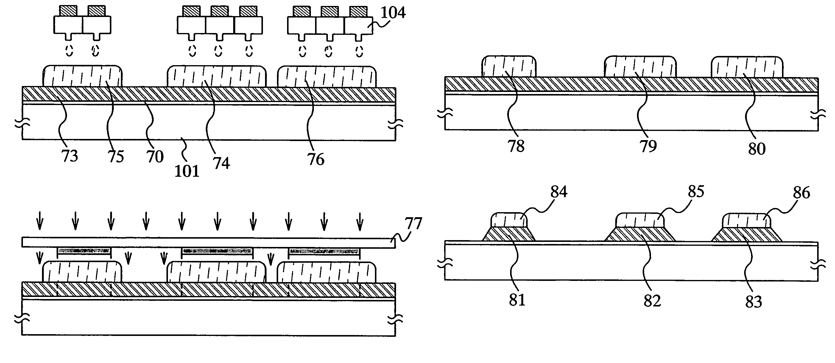
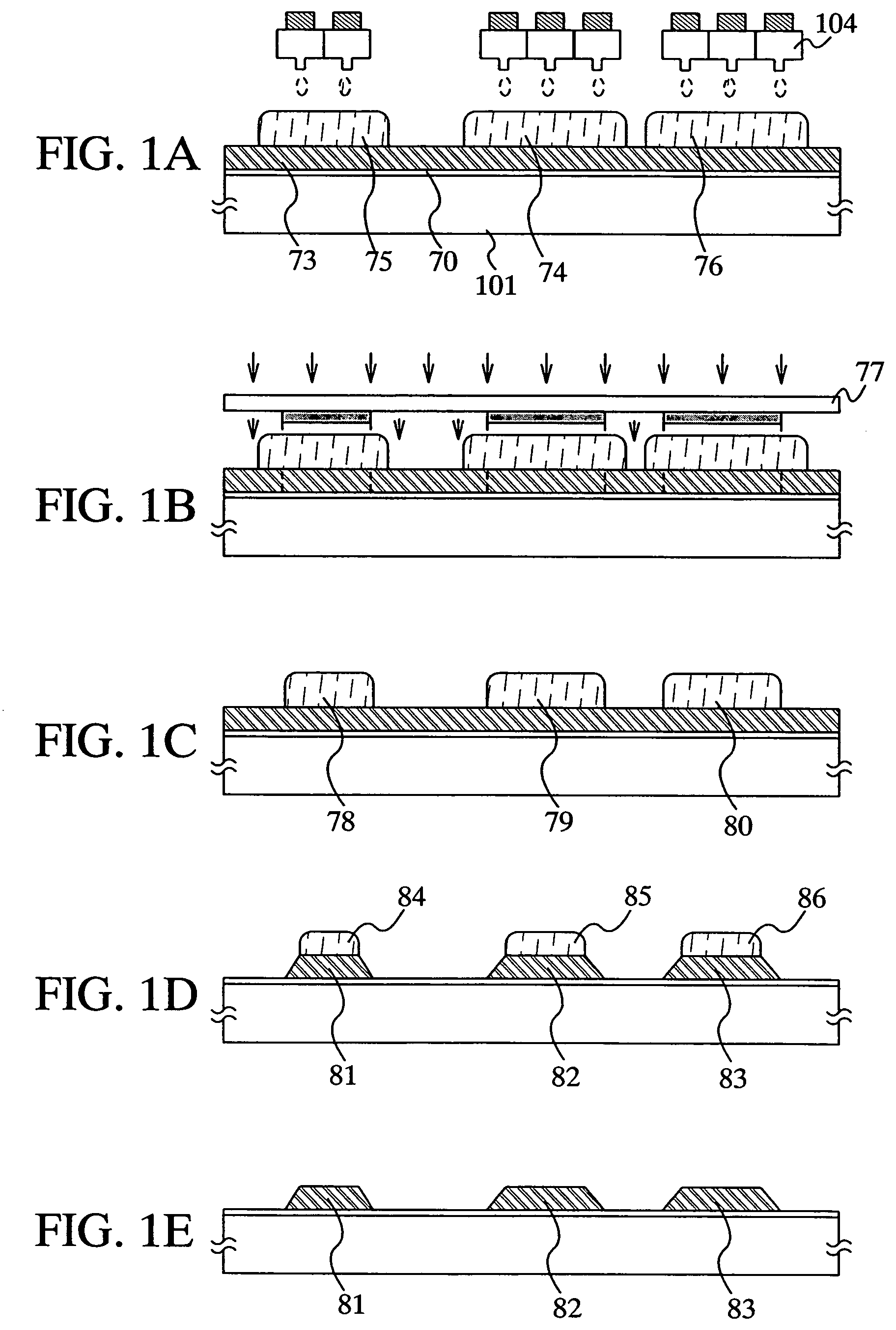
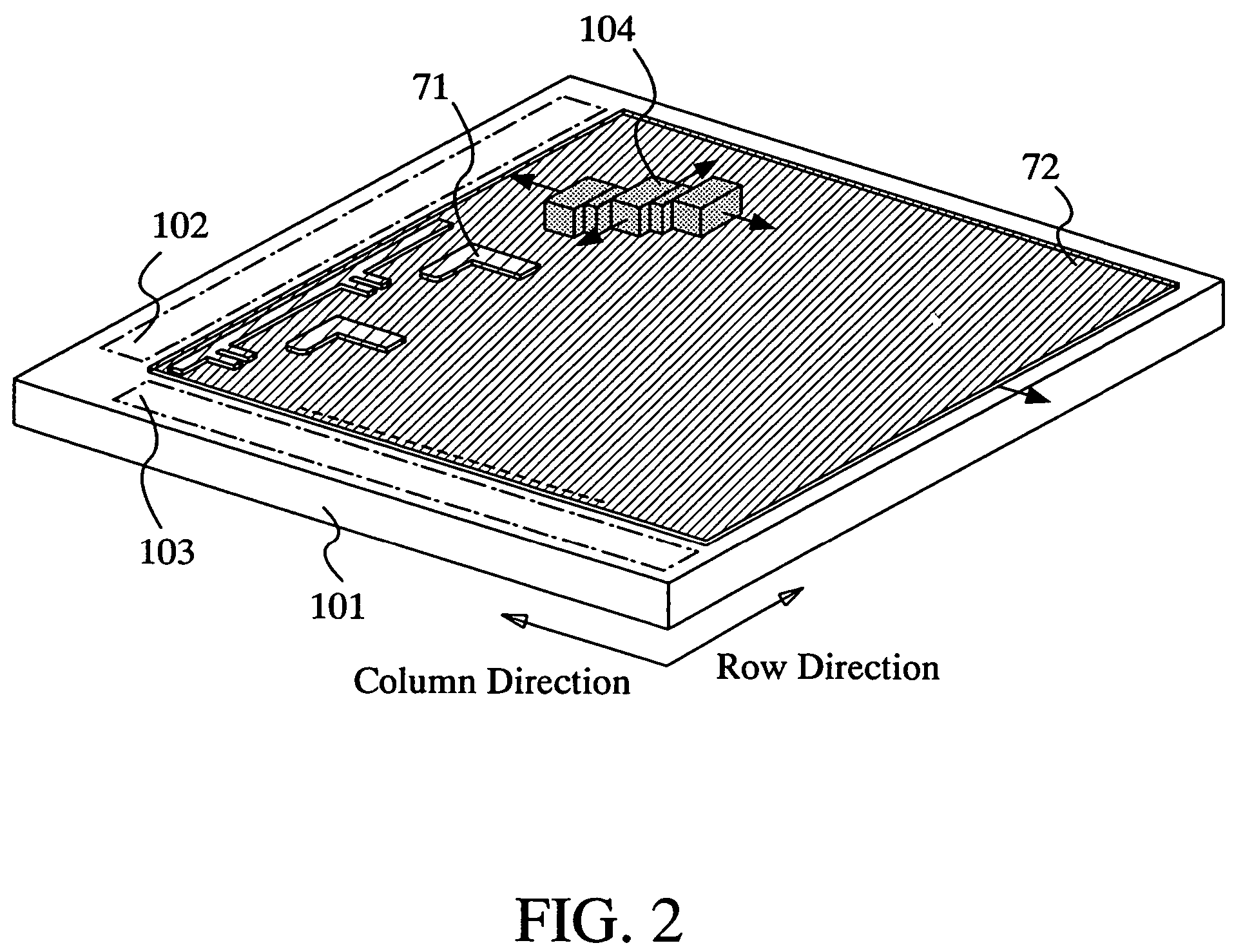
[0034]A mode of embodiment modes according to the present invention is described in detail with reference to FIGS. 1A to 3C. According to the present invention, a substrate 101 is to be formed of various materials such as glass, quartz, a semiconductor, a plastic, a plastic film, metal, a glass epoxy resin, and ceramic. The present invention can be applied to all step...

embodiment mode 2

[0051]In the embodiment mode, a liquid crystal display panel that is formed of a transistor composed of amorphous silicon using the present invention is described with reference to drawings. According to the embodiment mode, a method for manufacturing a resist pattern of the present invention is applied so as to form a gate electrode.

[0052]A substrate 101 is formed of various materials such as glass, quartz, a semiconductor, a plastic, a plastic film, metal, a glass epoxy resin, and ceramic. A conductive film 550 is formed of a material having a conductive material by using plasma CVD or sputtering so as to cover the substrate 101. (FIG. 12A)

[0053]A photoresist (photosensitive resin) that is sensitive to ultraviolet rays is applied on the conductive film 550 by an ink jetting under reduced pressure to form resists 551 and 552. (FIG. 12B) Since a step of spin coating is not required in the present invention in which the resist is formed by the ink jetting, efficiency in the use of a ...

embodiment 1

[0097]Embodiment of the present invention is described with reference to FIGS. 4 to 6. FIG. 4 shows a structure of a printer using ink jetting.

[0098]As shown in FIG. 4, the discharging period and the movement speed of a substrate 215 are regulated so as to continuously form a resist pattern from a composition discharged from an ink head 201 on the substrate. A nozzle 202 for discharging gas may be provided adjacent to the ink head 201 as a means of smoothing the composition. Using the gas discharged from the nozzle 202, the composition discharged over the substrate 215 is smoothed. A linear pattern is formed by relatively moving the ink head 201 and the substrate, at this time; the pattern can be smoothed by discharging the gas from the nozzle. Further, a gap between the ink head 201 and the substrate 215 is preferably maintained at a distance equal to or less than 1 mm in order to increase accuracy of a impact position of the discharged composition. To that end, a structure in whic...


PUM

PropertyMeasurementUnit
wavelengthaaaaaaaaaa
pressureaaaaaaaaaa
pressureaaaaaaaaaa

Abstract

To provide a method for manufacturing a resist pattern designed to reduce a manufacturing cost by improving efficiency in the use of a resist material, a method for removing a resist pattern, and a method for manufacturing a semiconductor device.
The present invention includes a step of forming a resist pattern by discharging a composition containing photosensitizer on a object to be processed under reduced pressure. The present invention includes a step of etching the object to be processed using the resist pattern as a mask, a step of irradiating the resist pattern through a photomask with light within a photosensitive wavelength region of a photosensitizer, and a step of removing the resist pattern on the object to be processed.

Description

BACKGROUND OF THE INVENTION[0001]1. Field of the Invention[0002]The present invention relates to a method for manufacturing a resist pattern, more particularly, the invention relates to a method for manufacturing a resist pattern by using ink jetting, a method for removing the resist pattern, and a method for manufacturing a semiconductor device.[0003]Further, the invention relates to a method for manufacturing a resist pattern by using a method for discharging a composition, a method for removing the resist pattern, and a method for manufacturing a semiconductor device.[0004]2. Description of the Related Art[0005]A thin film transistor (hereinafter referred to as a TFT) formed by using a thin film on an insulating surface is widely applied to an integrated circuit and the like, and is often used as a switching element. A display panel using the TFT has been widely used for a portable terminal and a large sized display device, therefore, high definition, high aperture ratio, high re...

Claims


Application Information

Patent Timeline
Patent Type & Authority Patents(United States)
IPC IPC(8): G03F7/20G03F7/16G03F7/26G03F7/00H01L21/77H01L21/84H01L27/12
CPCG03F7/0007H01L27/1288H01L27/1214G03F7/16
Inventor YAMAZAKI, SHUNPEIARAI, YASUYUKIWATANABE, YASUKO
Owner SEMICON ENERGY LAB CO LTD
Why Eureka
Try Eureka