Current-limiting diode
A diode and drain technology, which is applied in the field of power semiconductors, can solve the problem that gallium nitride heterojunction material power diodes have not received enough attention, and achieve the effect of avoiding lattice damage and reducing adverse effects.
Active Publication Date: 2017-12-22
UNIV OF ELECTRONICS SCI & TECH OF CHINA
View PDF7 Cites 6 Cited by
- Summary
- Abstract
- Description
- Claims
- Application Information
AI Technical Summary
Problems solved by technology
However, GaN heterojunction material power diodes have not received enough attention, especially GaN current-limiting diodes
Method used
View moreImage
Smart ImageViewing Examples

Examples
Embodiment Construction
[0021] The present invention has been described in detail in the part of the summary of the invention, and will not be repeated here.
Login to View More PUM
 Abstract
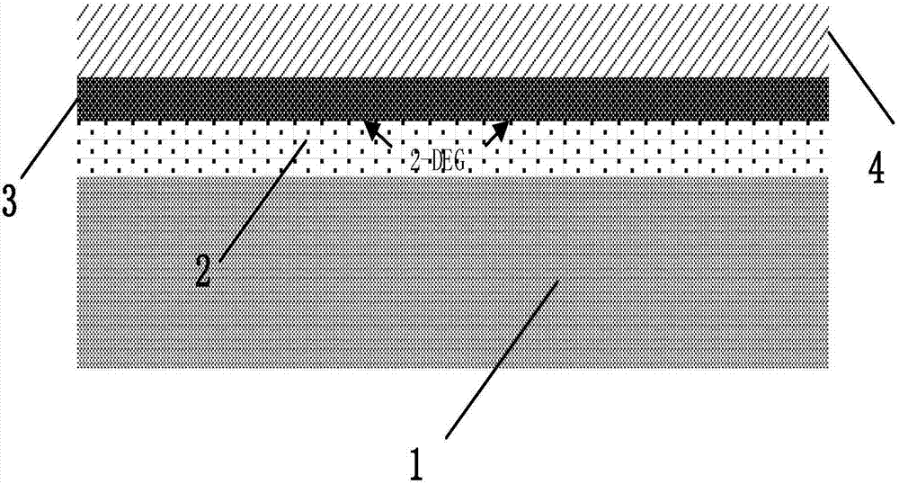
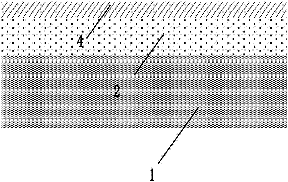
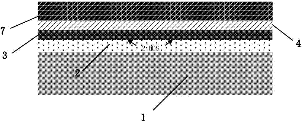
The invention belongs to the technical field of semiconductors, and relates to a current-limiting diode. The invention proposes the novel current-limiting diode, and the diode employs the technology of growing a charge restoration layer on a thin carrier AlGaN / GaN heterojunction to modulate two-dimensional electron gas. The structural advantages of the diode lie in that fluorine-based gas used for etching of the charge restoration layer can hardly cause any etching impact on a barrier layer below the charge restoration layer under the conditions that a device is enhanced and the diode has a lower start voltage and a large reverse withstand voltage, and finally can achieve the self-terminating at an AlGaN interface, so as to achieve the precise control of the barrier layer. The diode avoids the etching of the AlGaN layer, and cannot cause damages to the AlGaN layer, so the device is large in current density, is higher in electron mobility and is lower in conduction resistance.
Description
technical field [0001] The invention belongs to the technical field of power semiconductors and relates to a current-limiting diode. Background technique [0002] GaN power devices have become one of the best choices for the next generation of high-frequency and high-power devices due to their high reverse breakdown voltage, high carrier concentration formed by the high-voltage electric polarization effect, and high electron mobility. In recent years, AlGaN / GaN heterojunction enhanced HEMT devices have been extensively studied. However, GaN heterojunction material power diodes have not received enough attention, especially GaN current-limiting diodes. [0003] Due to the unprecedented development of the LED lighting industry, the demand for current limiting diodes (rectifiers) is also increasing. Current-limiting diodes are not only used to control the brightness of LED lighting, but also to protect power devices from damage caused by overcurrent and overload. [0004] Re...
Claims
Login to View More Application Information
Patent Timeline
 Patent Type & Authority Applications(China)
IPC IPC(8): H01L29/06H01L29/40H01L29/41H01L29/861
CPCH01L29/0684H01L29/402H01L29/41H01L29/8611
Inventor 周琦胡凯董长旭朱厉阳张波
Owner UNIV OF ELECTRONICS SCI & TECH OF CHINA