Seed crystal laying method, casting method of monocrystal silicon-like ingot and monocrystal silicon-like wafer

A laying method and a technology similar to single crystal silicon, which can be applied in the directions of single crystal growth, single crystal growth, chemical instruments and methods, etc., and can solve the problem of low reuse efficiency of seed crystals.

Inactive Publication Date: 2017-12-29
JINKO SOLAR CO LTD +1
View PDF6 Cites 8 Cited by
  • Summary
  • Abstract
  • Description
  • Claims
  • Application Information

AI Technical Summary

Problems solved by technology

[0005] Based on this, the embodiment of the present invention proposes a method for laying seed crystals, a method for casting quasi-single crystal silicon ingots, and a quasi-single crystal silicon wafer to solve the problem of low recycling efficiency of existing seed crystals

Method used


Image

  • Seed crystal laying method, casting method of monocrystal silicon-like ingot and monocrystal silicon-like wafer
  • Seed crystal laying method, casting method of monocrystal silicon-like ingot and monocrystal silicon-like wafer
  • Seed crystal laying method, casting method of monocrystal silicon-like ingot and monocrystal silicon-like wafer

Examples


Embodiment 1

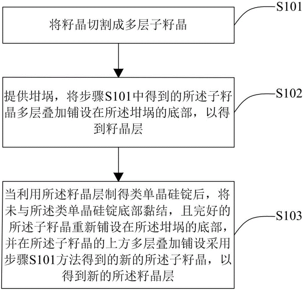
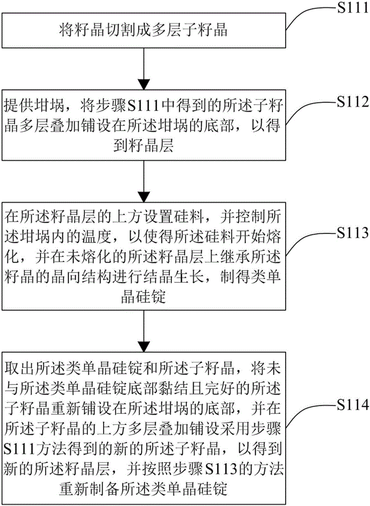
[0059] A method for laying a seed crystal for casting a quasi-single crystal, the method comprising:

[0060] (1) cutting the seed crystal with a length × width × height of 156 × 156 × 15 mm into three layers of sub-seeds, wherein the length × width × height of the cut sub-seeds is 156 × 156 × 5 mm;

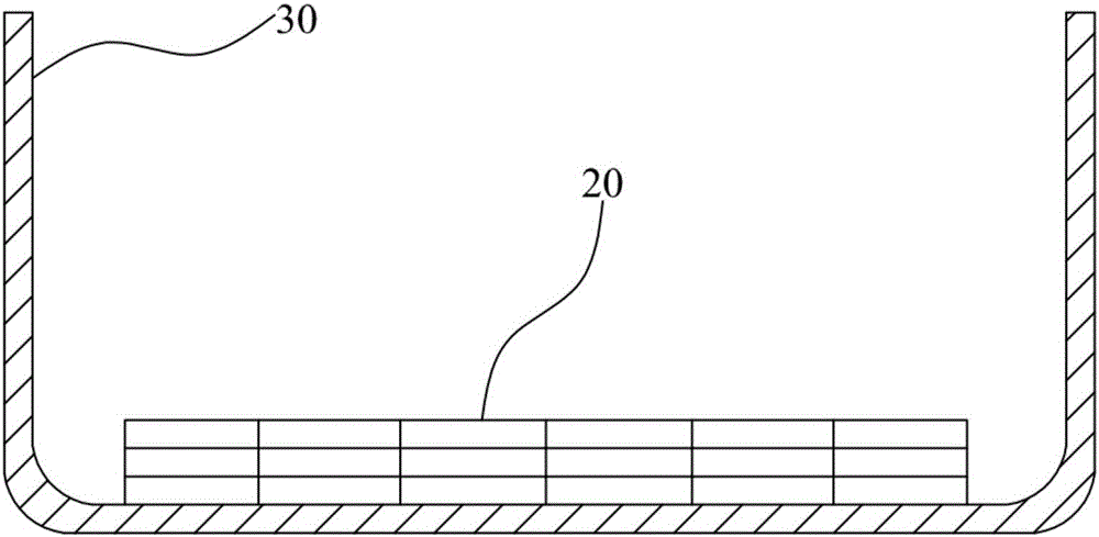
[0061] (2) Provide a crucible with an internal size of 1000×1000×480mm. The length×width×height obtained in step (1) is a total of 108 sub-seed crystals of 156×156×5mm. After splicing and laying a layer of sub-seeds in the arrangement of 6, sub-seeds in a 6×6 arrangement are further laid on the upper part of the sub-seeds in multiple layers, finally forming a three-layer 6×6 arrangement. The seed crystal layer formed by laying the sub-seed crystals, wherein each outer edge of the seed crystal layer maintains the same gap with the side wall of the crucible;

[0062] (3) After the quasi-single-crystal silicon ingot is produced by using the seed crystal layer, the sub-seed crystals...

Embodiment 2

[0065] A method for laying a seed crystal for casting a quasi-single crystal, the method comprising:

[0066] (1) cutting the seed crystal with a length × width × height of 156 × 156 × 15 mm into three layers of sub-seeds, wherein the length × width × height of the cut sub-seeds is 156 × 156 × 5 mm;

[0067] (2) Provide a crucible with an internal size of 840×840×460mm. The length×width×height obtained in step (1) is a total of 75 sub-seed crystals of 156×156×5mm. After splicing and laying a layer of sub-seeds in the arrangement of 5, sub-seeds in the arrangement of 5×5 are further laid on the upper part of the sub-seeds in multiple layers, finally forming a three-layer 5×5 arrangement. The seed crystal layer formed by laying the sub-seed crystals, wherein each outer edge of the seed crystal layer maintains the same gap with the side wall of the crucible;

[0068] (3) After the quasi-single-crystal silicon ingot is produced by using the seed layer, the sub-seed crystals that ...

Embodiment 3

[0070] A method for laying a seed crystal for casting a quasi-single crystal, the method comprising:

[0071] (1) cutting the seed crystal with a length × width × height of 156 × 156 × 16 mm into 4 layers of sub-seeds, wherein the length × width × height of the cut sub-seeds is 156 × 156 × 4 mm;

[0072] (2) Provide a crucible with an internal size of 1000×1000×480mm. The length×width×height obtained in step (1) is a total of 144 sub-seed crystals of 156×156×4mm. After splicing and laying a layer of sub-seeds in the arrangement of 6, sub-seeds in a 6×6 arrangement are further laid on the upper part of the sub-seeds in multiple layers, and finally form a four-layer 6×6 arrangement. The seed crystal layer formed by laying the sub-seed crystals, wherein each outer edge of the seed crystal layer maintains the same gap with the side wall of the crucible;

[0073] (3) After the quasi-single-crystal silicon ingot is produced by using the seed crystal layer, the sub-seed crystals tha...


PUM


Abstract

The invention discloses a seed crystal laying method, a casting method of a monocrystal silicon-like ingot and a monocrystal silicon-like wafer. The seed crystal laying method comprises the following steps: cutting seed crystal into multiple layers of sub seed crystal; providing a crucible, and stacking and laying the multiple layers of sub seed crystal at the bottom part of the crucible, thus obtaining a seed crystal layer; after preparing the monocrystal silicon-like ingot by utilizing the seed crystal layer, laying complete sub seed crystal which is not adhered to the bottom part of the monocrystal silicon-like ingot at the bottom part of the crucible again, and stacking and laying multiple layers of new sub seed crystal above the sub seed crystal, thus obtaining a new seed crystal layer. According to the seed crystal laying method disclosed by the invention, the seed crystal layer is formed by cutting the seed crystal into multiple layers of sub seed crystal and laying the multiple layers of sub seed crystal at the bottom part of the crucible; after preparation of the monocrystal silicon-like ingot is carried out, complete sub seed crystal in the seed crystal layer can be laid at the bottom part of the crucible again, and the new seed crystal layer can be obtained just by stacking and laying a part of new sub seed crystal above the complete sub seed crystal, so that the problem that the repeated utilization efficiency of existing seed crystal is not high is solved.

Description

technical field [0001] The invention relates to the technical field of semiconductor manufacturing, in particular to a method for laying seed crystals, a method for casting quasi-single crystal silicon ingots and quasi-single crystal silicon wafers. Background technique [0002] Solar energy is abundant and widely distributed, and it is the renewable energy with the greatest development potential. With the increasingly serious problems of global energy shortage and environmental pollution, solar photovoltaic power generation has become an emerging industry that is generally concerned and focused on development by countries all over the world due to its clean, safe, convenient and efficient features. According to the forecast of the European Photovoltaic Industry Association EPIA, solar photovoltaic power generation will occupy an important seat in the world's energy consumption in the 21st century. It is estimated that by 2030, the proportion of solar photovoltaic power gene...

Claims


Application Information

Patent Timeline
IPC IPC(8): C30B11/14C30B29/06
CPCC30B11/14C30B29/06
Inventor 李林东罗丁陈伟丁云飞严军辉金浩
Owner JINKO SOLAR CO LTD
Why Eureka
Try Eureka