Method for positioning failure of power device

A power device and failure location technology, which is applied in radiation pyrometry, instruments, scientific instruments, etc., can solve problems such as increased leakage current and shortened service life of devices, and achieves design cost reduction, fast response speed, and high sensitivity Effect

Inactive Publication Date: 2018-01-05
SHANGHAI RES INST OF MICROELECTRONICS SHRIME PEKING UNIV
View PDF6 Cites 8 Cited by
  • Summary
  • Abstract
  • Description
  • Claims
  • Application Information

AI Technical Summary

Problems solved by technology

The types of defects that cause increased leakage current include ESD, Latch-up, interjunction leakage current, hot carrier effect, gate oxide leakage current, etc.
The failure of the leakage current of the power chip will greatly shorten the service life of the device. Therefore, how to better locate and analyze the leakage current of the power device and improve its reliability has become a very important issue.

Method used


Image

  • Method for positioning failure of power device
  • Method for positioning failure of power device

Examples


Embodiment Construction

[0017] Below in conjunction with accompanying drawing, specific embodiment of the present invention is described further:

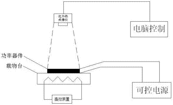
[0018] like figure 1 As shown, the equipment used in the power device failure location method described in the patent of the present invention consists of a stage with a temperature control device, an infrared thermal imager connected to a computer, and an external controllable power supply.

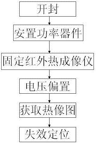
[0019] like figure 2 As shown, the patent of the present invention is a failure location method for power devices. Include the following steps:

[0020] Step 1: For power devices in non-hermetic epoxy molding compound packages, chemical corrosion is used for unsealing, while for power devices in hermetic epoxy molding compound packages or metal packages, mechanical methods are used for unsealing. The principle is not to destroy the electrical connection of the power device, and the goal is to completely expose the upper surface of the chip.

[0021] Step 2: Pla...


PUM


Abstract

The invention relates to the technical field of failure analysis for a power device, and relates to a method for positioning a failure of a power device. The increase of leakage current is one of themain electrical representation forms of a failure of the power device, and the service life of the device is greatly reduced. The invention provides a method for positioning a failure of the power device. The method comprises the steps of unpackaging a failure power device sample; placing the unpackaged power device on an object stage; fixing and adjusting an infrared thermal imager so as to enable a display screen of the infrared thermal imager to just accommodate a chip; performing voltage bias on the power device to find bias voltage with the hotspot being the clearest; applying the constant bias voltage to the power device, and acquiring a surface thermogram of the chip; and superimposing the thermogram and a physical structure diagram of the chip so as to accurately position abnormalleakage current. The method is convenient to implement, and can accurately capture a hotspot and position the failure location.

Description

technical field [0001] The invention relates to the technical field of chip-level failure analysis of power devices, in particular to a failure location method for power devices. Background technique [0002] Power devices are widely used in consumer goods, industry, medical and transportation industries, and are the main products of green energy, energy saving and environmental protection. Ensuring and improving the quality and reliability of devices is a very important topic. Excellent device quality requires repeated improvements in the stages of design, process and product development, mass production, reliability testing, and packaging. These are inseparable from failure analysis, and even when the product enters the system application end, there is also a need for failure analysis. [0003] The chip-level and package-level stages of power devices determine the quality of the product most. The failure analysis at the package level will be carried out in combination wit...

Claims


Application Information

Patent Timeline
Patent Type & Authority Applications(China)
IPC IPC(8): G01R31/28G01R31/02G01J5/00
Inventor 沈立程玉华
Owner SHANGHAI RES INST OF MICROELECTRONICS SHRIME PEKING UNIV
Why Eureka
Try Eureka