Chip package structure and package method

A chip packaging structure and chip packaging technology, applied in the direction of electrical components, electric solid devices, circuits, etc., can solve the problems of high preparation cost of lead frame structure, labor and time cost, unfavorable heat dissipation at the bottom of the chip, etc., to achieve the advantage of fixing Effects of connection, simplification of packaging process, and prevention of shifting or dropping

Active Publication Date: 2018-01-09
NAT CENT FOR ADVANCED PACKAGING
View PDF6 Cites 1 Cited by
  • Summary
  • Abstract
  • Description
  • Claims
  • Application Information

AI Technical Summary

Problems solved by technology

[0004] The above-mentioned QFN packaging structure has the following defects: 1. A lead frame structure needs to be formed before packaging, and the preparation cost of the lead frame structure is relatively high, and the process is relatively complicated; 2. The lead frame structure is located at the bottom of the chip, and the overall package thickness is relatively large, and It is not conducive to the heat dissipation at the bottom of the chip; 3. When packaging the chip, each contact electrode of each chip needs to be connected to the lead frame frame, which consumes a lot of manpower and time costs; 4. In the patch or wire bonding process It is easy to cause problems such as deformation of the lead frame frame, which affects the yield of the overall packaged chip

Method used


Image

  • Chip package structure and package method
  • Chip package structure and package method
  • Chip package structure and package method

Examples


Embodiment 1

[0056] This embodiment provides a chip packaging method, such as Figure 1-12 shown, including the following steps:

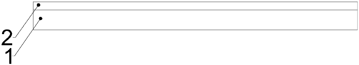
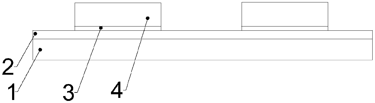
[0057] Step S1, providing a carrier 1, the carrier 1 is selected from but not limited to glass or stainless steel.

[0058] Step S2 , forming a first adhesive layer 2 on the carrier 1 , specifically, spin-coating a photosensitive temporary bonding glue, such as UV glue, etc. on the carrier 1 by spin coating. When the carrier board 1 is made of stainless steel, a heat-peelable film can also be provided on the carrier board 1 as the first adhesive layer 2; a second adhesive layer 3 is formed on the bottom of several chips 4 to be packaged. As an embodiment of the present invention, in this embodiment, specifically, a DAF adhesive film is provided on the bottom of the chip 4 to be packaged.

[0059] The formation of the first adhesive layer 2 and the second adhesive layer 3 is conducive to the fixed connection between the subsequent chip 4 and the carrier 1, pre...

Embodiment 2

[0088] This embodiment provides a chip packaging structure, such as Figure 9 As shown, it includes a carrier board 1 , a connector 5 , a plastic package 7 and a conductive layer 9 .

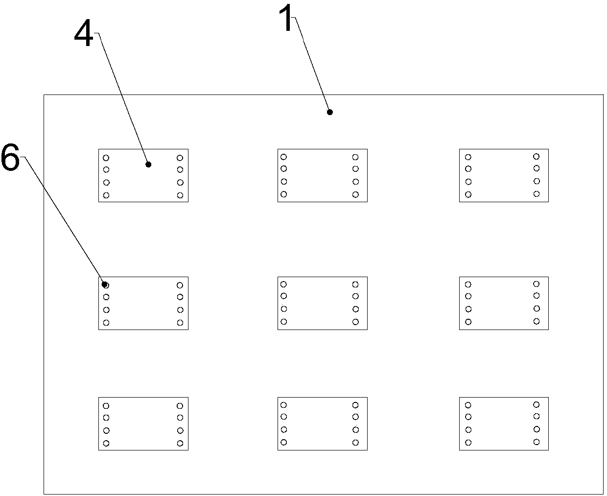
[0089] The carrier 1 is used to place several chips 4, the carrier 1 is selected from but not limited to glass or stainless steel, and the chips 4 are arranged in a matrix and distributed on the carrier 1;

[0090] The connector 5 is used to connect adjacent chips 4, specifically, the connector 5 is a bonding wire, which can be a gold wire or a silver wire, and the connector 5 protrudes outward in an arched shape;

[0091] The plastic package 7 is used to wrap the chip 4 and the connector 5, and expose the top of the connector 5. The exposed area can be determined according to the actual situation, wherein the material of the plastic package 7 is powder resin or liquid resin;

[0092] The conductive layer 9 is used to cover the exposed area on the top of the connector 5 and also covers part of ...


PUM


Abstract

The invention relates to the technical field of chip package, and discloses a chip package method. The chip package method comprises the steps of providing a carrying plate; positively arranging a plurality of chips on the carrying plate; electrically connecting adjacent chips by a bonding wire; packaging the chips and the bonding wires to form a plastic package body by a plastic package process,and allowing the bonding wires to be at least partially exposed; and forming a conductor layer on a region, where the bonding wires are exposed, of a surface of the plastic package body. By the chip package method, a wire rack of a metal material is not needed to be fabricated in advance, the cost is reduced, the fabrication process of the wire rack is saved, the process of arranging the wire rackunder the chips is omitted, the package process is effectively simplified, the package difficulty is reduced, the package efficiency is improved, the problem that the wire rack is deformed caused byprocesses such as surface mounting and bonding during the traditional package process is prevented, and the product yield is remarkably improved.

Description

technical field [0001] The invention relates to the technical field of chip packaging, in particular to a chip packaging structure and a packaging method. Background technique [0002] QFN (Quad Flat No-lead Package), is one of the surface mount packages, because of its good electrical and thermal performance, small size and light weight, it has been more and more widely used Applications. Generally, the QFN package structure is square or rectangular. There is a large-area exposed pad for heat conduction at the center of the bottom of the package, and there are conductive pads for electrical connection on the periphery of the package surrounding the large pad. [0003] The prior art discloses a QFN packaging structure, which includes a lead frame structure, a semiconductor chip and a packaging unit. The lead frame structure includes a base, a plurality of terminals and a first metal layer, and the base has a central area for To carry a semiconductor chip, and a peripheral ...

Claims


Application Information

Patent Timeline
IPC IPC(8): H01L23/538H01L23/31H01L21/56H01L23/498
CPCH01L2224/48137
Inventor 刘军
Owner NAT CENT FOR ADVANCED PACKAGING
Why Eureka
Try Eureka