Preparation method for HfS2 signal crystal nanosheet

A single crystal nano, substrate technology, applied in the direction of single crystal growth, nanotechnology, single crystal growth, etc., can solve the problems of limiting HfS research, low yield, difficult to control the number of layers, etc.

Active Publication Date: 2018-01-12
UNIV OF ELECTRONICS SCI & TECH OF CHINA
View PDF5 Cites 5 Cited by
  • Summary
  • Abstract
  • Description
  • Claims
  • Application Information

AI Technical Summary

Problems solved by technology

However, the above studies are all based on the HfS obtained by the mechanical exfoliation method. 2 , the few-layer HfS obtained by mechanical exfoliation is difficult to control 2 The number of layers, while the yield is very low, greatly limits the ability of HfS 2 Research

Method used


Image

  • Preparation method for HfS2 signal crystal nanosheet
  • Preparation method for HfS2 signal crystal nanosheet
  • Preparation method for HfS2 signal crystal nanosheet

Examples


Embodiment 1

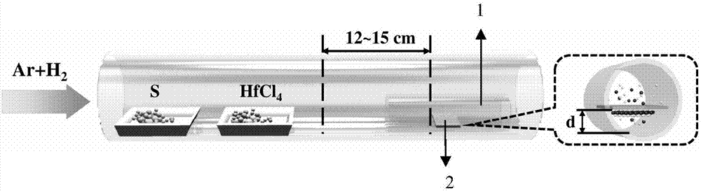
[0032] a HfS 2 A method for preparing a single crystal nanosheet, comprising the following steps:

[0033] Step 1: Put the S source and the Hf source in the upstream area of ​​the quartz tube, place the embedded quartz tube with an inner diameter of 12mm in the downstream area, place the mica substrate in the embedded quartz tube, and place it at a distance of 13cm from the heating center of the quartz tube;

[0034] Step 2: Vacuumize the inside of the quartz tube to 1Pa, and pass Ar gas to remove the residual air in the tube and keep the air pressure in the tube at normal pressure; then pass 15 sccm of Ar and 5 sccm of H into the tube 2 Respectively as carrier gas and shielding gas;

[0035] Step 3: Heat HfCl at 330°C and 220°C respectively 4 and S powder until evaporation, under the condition that the heating center temperature of the quartz tube is 900°C, and the distance d between the mica substrate and the lower wall of the embedded quartz tube is 1.5 mm, react for 10 m...

Embodiment 2

[0039] Example 2. HfS 2 Preparation of Single Crystal Nanosheets

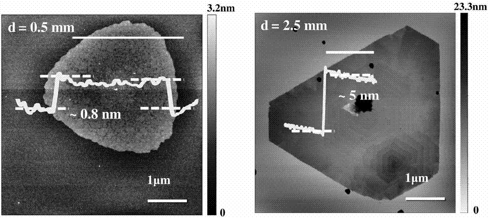
[0040] Prepare HfS according to the steps of Example 1 2 For single crystal nanosheets, the distance d between the mica substrate and the lower wall of the embedded quartz tube in the confinement space is 0.5mm and 2.5mm respectively, and other steps remain unchanged. HfS obtained under this example 2 Atomic force microscope image of a single crystal nanosheet image 3 shown.

Embodiment 3

[0041] Example 3. HfS 2 Preparation of Single Crystal Nanosheets

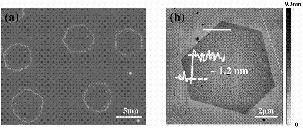
[0042] Prepare HfS according to the steps of Example 1 2 For single crystal nanosheets, the reaction temperatures were changed to 800°C, 850°C, 940°C and 980°C, respectively, and other steps remained unchanged. HfS obtained under this embodiment 2 The atomic force microscope image of single crystal nanosheets and the statistics of thickness and nucleation density are shown in Figure 5 shown.


PUM

PropertyMeasurementUnit
thicknessaaaaaaaaaa

Abstract

The invention discloses a preparation method for a HfS2 single crystal nanosheet, and belongs to the field of preparation of semiconductor materials. The method comprises the following steps: (1) putting an S source and an Hf source in an upstream area of a quartz tube, placing an embedded quartz tube of which an inner diameter is smaller than that of the quartz tube in a downstream area, and placing a mica substrate into the embedded quartz tube; (2) performing vacuumizing on the interior of the quartz tube, introducing an inert gas to make pressure in the tube keep an atmospheric pressure environment, and introducing a carrier gas flow and a protective gas; and 3) heating the S source and the Hf source to evaporation, performing a reaction for 5-15 minutes under conditions that the temperature is 800-980 DEG C, a distance d between the mica substrate and the lower wall of the embedded quartz tube is 0.5-2.5mm, performing natural cooling on the quartz tube to a room temperature, and taking out the substrate. According to the invention, parameters such as the distance d between the mica substrate and the lower wall of the embedded quartz tube and a deposition temperature are optimized, thus controllable growth of the HfS2 nanosheet with a thickness of 0.8-15nm and a side length of about 5 micrometers is realized.

Description

technical field [0001] The invention belongs to the technical field of preparation of semiconductor materials, in particular to a HfS 2 Preparation method and application of single crystal nanosheets. Background technique [0002] In recent years, ultra-thin two-dimensional materials with atomic-level thickness have received extensive attention, especially transition metal sulfides, because of their unique physical and chemical properties and certain band gaps, they have great significance in the fields of micro-nano electronics and photodetection. application prospects. Two-dimensional materials with high mobility are suitable for various micro-nano electronic devices, and play an important role in promoting the development of the semiconductor device industry. [0003] Hf 2 It is a transition metal sulfide of group IVB, and its interlayer forms a layered structure through the extremely weak Van der Waals force, the interlayer distance is about 0.59nm, and each layer is ...

Claims


Application Information

Patent Timeline
Patent Type & Authority Applications(China)
IPC IPC(8): C30B25/00C30B29/46C30B29/60B82Y15/00B82Y30/00B82Y40/00
Inventor 熊杰晏超贻邬春阳龚传辉戴丽萍李言荣
Owner UNIV OF ELECTRONICS SCI & TECH OF CHINA
Why Eureka
Try Eureka