Supercharge Your Innovation With Domain-Expert AI Agents!

Manufacturing method for multilayer structure for image display device

A technology of an image display device and a manufacturing method, which are applied in the directions of identification devices, films/sheets without carriers, and film/sheet adhesives, etc., can solve problems such as difficulty, and achieve the effect of reliable bonding

Active Publication Date: 2018-01-19
MITSUBISHI CHEM CORP
View PDF7 Cites 0 Cited by
  • Summary
  • Abstract
  • Description
  • Claims
  • Application Information

AI Technical Summary

Problems solved by technology

However, it is not easy to bond the image display panel and the front panel with a single adhesive sheet without gaps

Method used


Image

  • Manufacturing method for multilayer structure for image display device
  • Manufacturing method for multilayer structure for image display device
  • Manufacturing method for multilayer structure for image display device

Examples


Embodiment 1

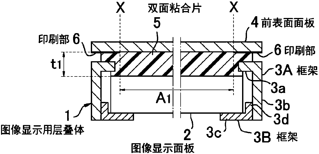
[0225] In the present example, after preparing the adhesive composition, a double-sided adhesive sheet was prepared so as to satisfy [Formula 1], and then, the front edge of the frame was sandwiched between the image display panel and the front panel. Between, and sandwiching the double-sided adhesive sheet, the aforementioned image display panel and the aforementioned front panel are stacked to form a laminated body, and then the aforementioned laminated body is heated to soften the aforementioned double-sided adhesive sheet, and then, by irradiating The active energy ray crosslinks the double-sided pressure-sensitive adhesive sheet to bond the image display panel and the front panel, thereby producing a laminate for an image display device.

[0226] The description will be given in order below.

[0227] (synthesis of macromers)

[0228] Add 900 parts by mass of deionized water, 60 parts by mass of 2-sulfoethyl sodium methacrylate, 10 parts by mass of potassium methacrylate ...

Embodiment 2

[0251] The laminated body 1 for image display apparatuses was produced similarly to Example 1 except having made the dimension of the double-sided adhesive sheet α into 293 mm x 180 mm, and thickness 0.5 mm.

Embodiment 3

[0253] Prepare 50 parts by weight of 2-ethylhexyl acrylate (homopolymer Tg (glass transition point of polymer obtained by polymerizing only 2-ethylhexyl acrylate): -70°C), 45 parts by weight of vinyl acetate Acrylate copolymer (A-2) (Mn=65400, Mw=167000, Mw / Mn=2.56). 70 g of UV-curable resin propoxylated pentaerythritol triacrylate ("ATM-4PL" manufactured by Shin-Nakamura Industry Co., Ltd.) 15 g of 4-methylbenzophenone to prepare adhesive composition b.

[0254] Instead of the PSA composition a used in Example 1, the above-mentioned PSA composition b was used to produce a double-sided PSA sheet β.

[0255] It was confirmed that the double-sided PSA sheet β has a glass transition temperature (Tg) of 10°C, softens when heated to 60-100°C, and is irradiated with a high-pressure mercury lamp with a cumulative light intensity of 2000mJ / cm on one side. 2 When cross-linking with ultraviolet energy (converted to a wavelength of 365 mm), the holding force measured in the holding f...


PUM

PropertyMeasurementUnit
glass transition temperatureaaaaaaaaaa
thicknessaaaaaaaaaa

Abstract

Proposed is a manufacturing method for a multilayer structure for an image display device, the multilayer structure being formed by interposing at least a portion of a frame (3) between a screen display panel (2) and a front surface panel (4) and affixing the screen display panel and the front surface panel with a double-sided adhesive sheet (5), wherein: the double-sided adhesive sheet is designed so that a prescribed formula is satisfied by the thickness and area of the double-sided adhesive sheet prior to affixing, and the maximum thickness of the double-sided adhesive sheet after fixing and the area of the valid image display surface of the image display panel; and the manufacturing method includes the following steps. (a) A step for producing a double-sided adhesive sheet by molding,into a sheet shape, an adhesive compound which was crosslinked by active energy ray projection. (b) A step for producing a multilayer structure by interposing the frame between the screen display panel and the front surface panel and stacking the screen display panel and the front surface panel with the double-sided adhesive sheet interposed therebetween. (c) A step for softening the double-sidedadhesive sheet. (d) A step for projecting active energy rays onto the double-sided adhesive sheet.

Description

technical field [0001] This invention relates to the manufacturing method of the laminated body for image display apparatuses provided with the structure which bonded the image display panel and the front panel with the adhesive sheet. Background technique [0002] A liquid crystal display as an example of an image display device, such as image 3 As shown, the liquid crystal device (LCD) 101 is generally constructed by arranging a backlight unit for illuminating the liquid crystal display panel on the back side of the liquid crystal display panel, and housing the liquid crystal device 101 in a case composed of LCD frames 103 and 104. Inside the body (also referred to as chassis), on the other hand, a front panel 102 such as a protective panel or a touch panel is disposed on the front side of the liquid crystal device 101 . At this time, in order to impart cushioning properties, specifically, for example, in order not to cause bleeding of the liquid crystal device (LCD) due ...

Claims


Application Information

Patent Timeline
Patent Type & Authority Applications(China)
IPC IPC(8): G09F9/00C09J7/00C09J133/04C09J151/00G02F1/1333C09J7/10
CPCC09J133/04C09J151/00G02F1/1333G09F9/00C09J2203/318C09J7/10C09J7/35G09F9/30
Inventor 山本亮太稻永诚内田贵久新美嘉穗儿
Owner MITSUBISHI CHEM CORP
Features
  • R&D
  • Intellectual Property
  • Life Sciences
  • Materials
  • Tech Scout
  • Unparalleled Data Quality
  • Higher Quality Content
  • 60% Fewer Hallucinations
Learn More