Compensation structure of driving circuit, driving circuit module and display panel

A technology of drive circuit and compensation structure, which is applied in the direction of static indicators and instruments, can solve the problems of low voltage value, easy interference of voltage signal, and higher and higher requirements for analog-to-digital conversion accuracy, so as to achieve calibration function and overcome Effects of reduced sensing voltage and shortened sensing time

Active Publication Date: 2020-02-28
BOE TECH GRP CO LTD
View PDF5 Cites 1 Cited by
  • Summary
  • Abstract
  • Description
  • Claims
  • Application Information

AI Technical Summary

Problems solved by technology

Although this voltage-type external compensation method has the advantages of fast driving speed and good compensation effect, the voltage signal is easily disturbed; in addition, with the increase in size and resolution, the parasitic capacitance of the display panel is getting larger and larger, and the fixed time The voltage value of the sensing (sense) pixel becomes lower, and the requirement for the accuracy of analog-to-digital conversion is getting higher and higher

Method used


Image

  • Compensation structure of driving circuit, driving circuit module and display panel
  • Compensation structure of driving circuit, driving circuit module and display panel
  • Compensation structure of driving circuit, driving circuit module and display panel

Examples


Embodiment 1

[0049] This embodiment aims at the problems existing in voltage-type external compensation, and provides a compensation structure for a current-type driving circuit. The compensation junction can effectively compensate the driving circuit and ensure compensation accuracy.

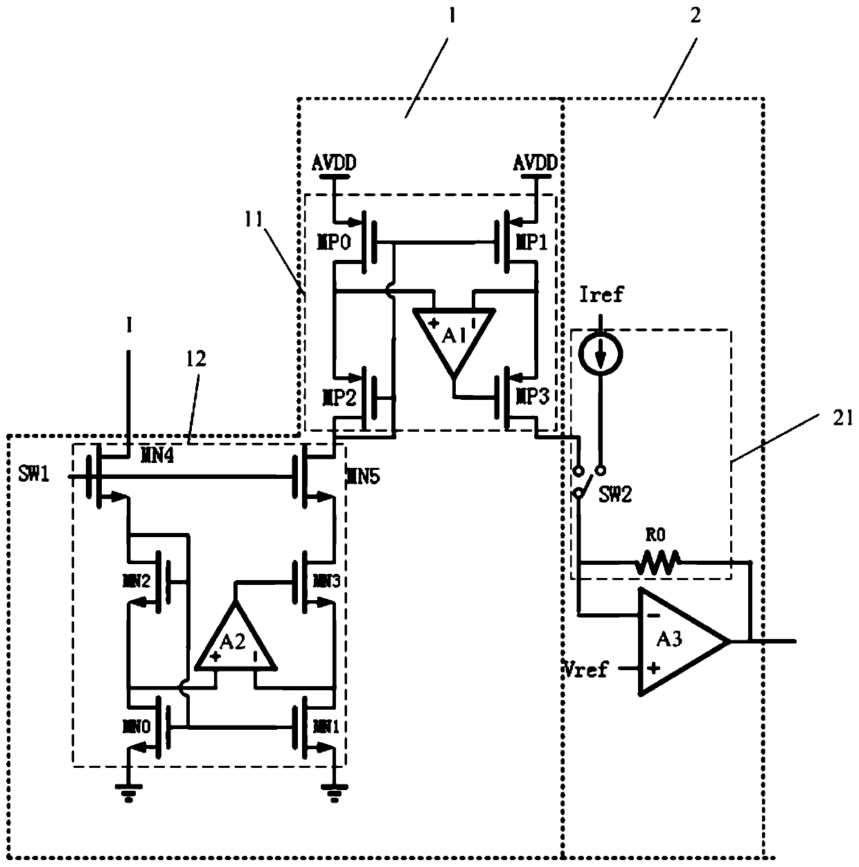
[0050] The compensation structure of the drive circuit is used to provide compensation current for the drive circuit, such as figure 1 As shown, it includes a current amplifying circuit 1 and a cross-group amplifying circuit 2, wherein:

[0051] The current amplification circuit 1 is connected to the output end of the driving circuit, and is used to amplify the driving current output by the driving circuit by a set factor;

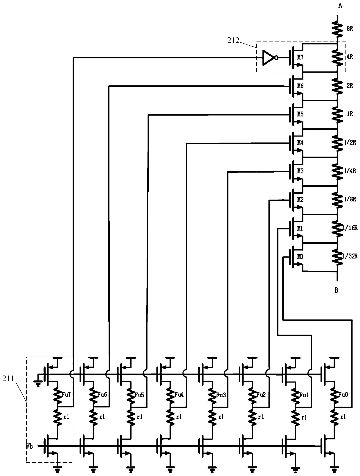
[0052] The cross-group amplifying circuit 2 is connected to the output terminal of the current amplifying circuit 1, and is used for matching the resistance in the compensation structure and converting the driving current into a corresponding driving voltage. Usually, an operational am...

Embodiment 2

[0087] This embodiment provides a driving circuit module, which includes a driving circuit and the compensation structure of the driving circuit in Embodiment 1, which has a better driving effect.

[0088] In the driving circuit module, there is no limitation on the structure of the driving circuit therein. As an example, such as Figure 4 As shown, the driving circuit 3 is a common 2T1C pixel circuit, and T1 is a scanning switch tube, which is responsible for writing the driving voltage data (Data) into the gate of the driving tube T2 row by row; T2 is the driving tube, which converts the voltage signal into Current is supplied to the OLED device. The gate of T1 is connected to the scan signal, the source is connected to Data data; the gate of T2 is connected to the drain of T1, the source is connected to OVDD, the drain is connected to the anode of OLED, the anode of the OLED device is connected to the drain of T2, and the cathode is grounded.

[0089] When the current-typ...

Embodiment 3

[0093] This embodiment provides a display panel, which further includes the compensation structure of the driving circuit in the second embodiment.

[0094] The display panel can be: desktop computer, tablet computer, notebook computer, mobile phone, PDA, GPS, vehicle display, projection display, video camera, digital camera, electronic watch, calculator, electronic instrument, instrument, LCD panel, electronic paper, TV Computers, monitors, digital photo frames, navigators and any other products or components with display functions can be applied to multiple fields such as public display and virtual display.


PUM


Abstract

The invention belongs to the technical field of display, and specifically relates to a compensation structure of a drive circuit, a drive circuit module and a display panel. The compensation structureof a drive circuit includes a current amplification circuit and a cross-group amplification circuit, wherein the current amplification circuit is connected with the output terminal of the drive circuit, and is used for amplifying the drive current output from the drive circuit by a set multiple; and the cross-group amplification circuit is connected with the output terminal of the current amplification circuit, and is used for matching different channels in the drive circuit and the resistors of different thin film transistors, and converting the drive current into the corresponding drive voltage. The compensation structure of a drive circuit can directly sense the drive current of the pixel data in the display panel, thus avoiding the problem that a voltage signal is easy to be interfered during the wiring process, improving the sensing accuracy and reducing the sensing time, and at the same time utilizes the cross-group amplification circuit and uses the fuse technology to perform fine tuning on the resistors of all the cross-group amplifiers so as to realize the calibration function, thus avoiding the problem of occurrence of process deviation.

Description

technical field [0001] The invention belongs to the field of display technology, and in particular relates to a compensation structure of a driving circuit, a driving circuit module and a display panel. Background technique [0002] LCD (Liquid Crystal Display, Liquid Crystal Display) and OLED (Organic Light-Emitting Diode: Organic Light-Emitting Diode) display devices have become popular flat panel display devices today. In particular, active matrix organic light emitting diodes (Active Matrix OLED, referred to as AMOLED) have been used in high-end TVs and mobile devices due to their advantages such as ultra-thin, high color gamut, high contrast, wide viewing angle, and fast response. [0003] AMOLED is a current mode (Current mode) active drive, which includes thin film transistors (Thin Film Transistor, referred to as TFT) for driving. Due to the deviation of the TFT process, the parameters such as the threshold voltage and electron mobility of each drive transistor may n...

Claims


Application Information

Patent Timeline
Patent Type & Authority Patents(China)
IPC IPC(8): G09G3/3241
Inventor 王糖祥宋琛
Owner BOE TECH GRP CO LTD
Why Eureka
Try Eureka