SiNx-Based optical reading synaptic device structure and preparation method thereof

A technology of synapse and device structure, applied in nanotechnology, electrical components, nanotechnology and other directions for materials and surface science, can solve the problem of not using photonic medium to read the weight of synapse, and achieve device size zoom out effect

Active Publication Date: 2018-01-26
UNIV OF ELECTRONICS SCI & TECH OF CHINA
View PDF3 Cites 9 Cited by
  • Summary
  • Abstract
  • Description
  • Claims
  • Application Information

AI Technical Summary

Problems solved by technology

However, so far, in the published patents of synaptic devices based on the memristive effect, all are based on electronic media to read synaptic weights, which can be called "electrically modulated electrical reading", and do not use photons. medium to read the weight of synapses (reference basis: CN 104916313 A, CN 10378055A, CN105287046A, CN105304813A, CN 104934534 A, CN104376362 A)

Method used


Image

  • SiNx-Based optical reading synaptic device structure and preparation method thereof

Examples


Embodiment Construction

[0029] Embodiments of the present invention are described below through specific examples, and those skilled in the art can easily understand other advantages and effects of the present invention from the content disclosed in this specification. The present invention can also be implemented or applied through other different specific implementation modes, and various modifications or changes can be made to the details in this specification based on different viewpoints and applications without departing from the spirit of the present invention.

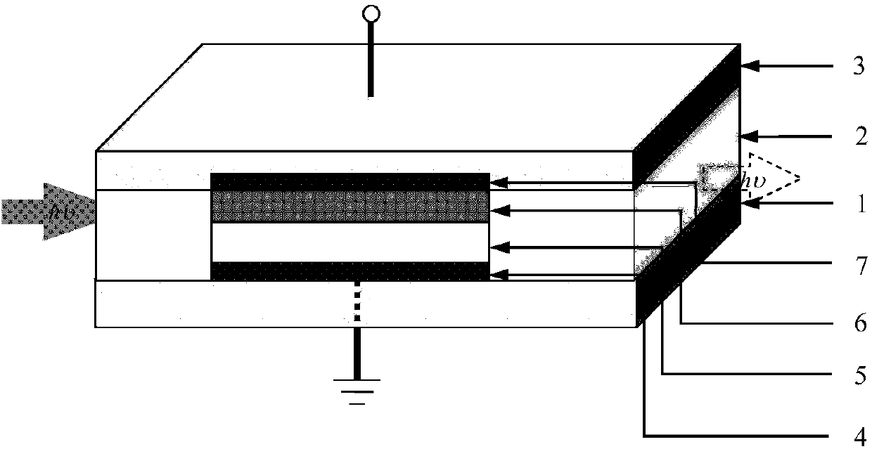
[0030] A SiN-based x Optically readable synaptic device structures, including "metal / SiN x / Metal" surface plasmon waveguide and embedded "top electrode / dual resistive variable layer / bottom electrode" memristor;

[0031] The surface plasmon waveguide has a vertical three-layer structure of "second metal layer 3 / dielectric layer 2 / first metal layer 1" from top to bottom;

[0032] The memristor has a vertical four-layer structure of "...


PUM

PropertyMeasurementUnit
thicknessaaaaaaaaaa
thicknessaaaaaaaaaa
thicknessaaaaaaaaaa

Abstract

The present invention provides a SiNx-Based optical reading synaptic device structure and a preparation method thereof. The SiNx-Based optical reading synaptic device structure includes a surface plasmon waveguide of a metal/SiNx/metal structure and a memristor of an upper electrode/dual-resistance varying layer/lower electrode structure; the surface plasmon waveguide is of a vertical three-layerstructure including a second metal layer, a dielectric layer and a first metal layer from top to bottom; the memristor is of a vertical four-layer structure including an upper electrode, a second resistance varying layer, a first resistance varying layer and a lower electrode from top to bottom; and the first resistance varying layer and the second resistance varying layer of the memristor, adopted as optical signal transmission channels, are horizontally connected with the dielectric layer of the surface plasmon waveguide. With the SiNx-Based optical reading synaptic device structure and thepreparation method thereof of the invention adopted, the optical reading of synaptic weight is realized, so that the optical reading synaptic device with the amplitude and phase of optical signals adopted as the synaptic weight has unparalleled advantages compared with a traditional synaptic device with resistance adopted as synaptic weight; and the surface plasmon waveguide can make the optical signals break through diffraction limits and transmitted, and therefore, the further reduction of the size of the device can be facilitated.

Description

technical field [0001] The invention belongs to the field of silicon-based photonic integrated devices and neuromorphic chips, in particular to a SiN-based x Optically readable neurosynaptic devices and methods of making the same. Background technique [0002] For a memristor with a "metal / dielectric layer / metal" sandwich structure, if different bias voltages are applied, the resistance of the device will show a nonlinear change. This non-linear change in resistance is caused by the formation or disappearance of conductive channels in the dielectric layer under different bias voltages. Interestingly, the connection strength of this nanoscale filamentous conductive channel varies with the magnitude and duration of the bias voltage. This property is very similar to the working mechanism of synapses connecting different neurons in the biological nervous system. It is this similarity between memristors and biological system synapses that makes them very suitable as synaptic d...

Claims


Application Information

Patent Timeline
Patent Type & Authority Applications(China)
IPC IPC(8): H01L45/00B82Y30/00
Inventor 李伟侯伟苟豪孟文林陈奕丞钟豪李东阳蒋亚东
Owner UNIV OF ELECTRONICS SCI & TECH OF CHINA
Why Eureka
Try Eureka