Organic optical waveguide embedded PCB processing method

A processing method and optical waveguide technology, applied in the direction of multi-layer circuit manufacturing, etc., can solve the problems such as the production method of organic optical waveguide embedded PCB, which is convenient for commercial promotion, improves alignment accuracy, and is suitable for large-scale The effect of production

Active Publication Date: 2018-01-30
SHENNAN CIRCUITS
View PDF11 Cites 1 Cited by
  • Summary
  • Abstract
  • Description
  • Claims
  • Application Information

AI Technical Summary

Problems solved by technology

[0004] Universities and scientific research institutes have conducted a large number of experiments, and the related optical waveguide system has become increasingly mature, but there is still no standard manufacturing method for organic optical waveguide embedded PCB

Method used


Image

  • Organic optical waveguide embedded PCB processing method
  • Organic optical waveguide embedded PCB processing method
  • Organic optical waveguide embedded PCB processing method

Examples


Embodiment 1

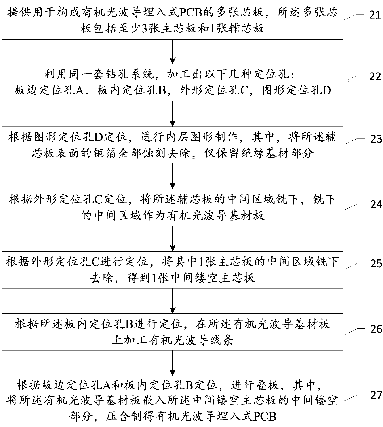
[0071] Please refer to figure 2 , this embodiment provides a method for processing an organic optical waveguide embedded PCB, using hole positioning to manufacture organic optical waveguide strips, the method may include:

[0072] 21. Provide multiple core boards for forming an organic optical waveguide embedded PCB, the multiple core boards include at least 3 main core boards and 1 auxiliary core board;

[0073] 22. Use the same drilling system to drill the multiple core boards, and process the following positioning holes: board edge positioning hole A for lamination positioning, for organic optical waveguide processing positioning and lamination Positioning hole B in the board for positioning, shape positioning hole C for positioning the inner core board milling shape, and graphic positioning hole D for making and positioning the inner layer of the core board;

[0074] 23. Perform positioning according to the pattern positioning hole D, and make inner layer patterns for th...

Embodiment 2

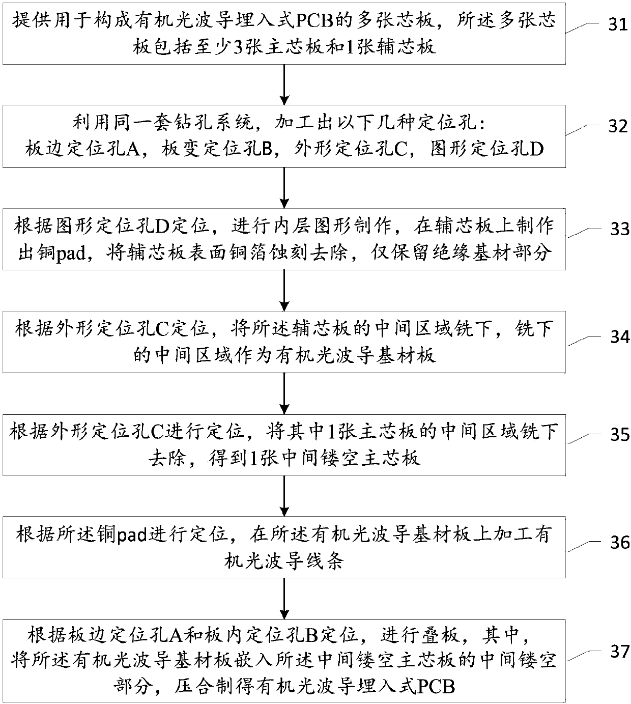
[0085] Please refer to image 3 , the present embodiment provides a method for processing an organic optical waveguide embedded PCB, using graphic positioning to manufacture organic optical waveguide strips, the method may include:

[0086] 31. Provide multiple core boards for forming an organic optical waveguide embedded PCB, the multiple core boards include at least 3 main core boards and 1 auxiliary core board;

[0087] 32. Use the same drilling system to drill the multiple core boards, and process the following positioning holes: board edge positioning hole A for lamination positioning and board inner positioning hole B for inner layer Shape positioning hole C for core board milling shape positioning, and graphic positioning hole D for core board inner layer graphics making and positioning;

[0088] 33. Perform positioning according to the pattern positioning hole D, and make inner layer patterns on the plurality of core boards, wherein a copper pad for processing and pos...


PUM


Abstract

The invention discloses an organic optical waveguide embedded PCB processing method. The method comprises the steps of providing a plurality of core boards, which comprises at least three main core boards and one auxiliary core board; drilling and processing the plurality of core boards by using the same set of drilling system to bore board edge positioning holes, in-board positioning holes, profile positioning holes and graph positioning holes; manufacturing the inner layer graph according to the graph positioning holes, milling the central region of the auxiliary core board to serve as an organic optical waveguide substrate according to the profile positioning holes, milling and removing the central region of one main core board to obtain a main core board with a hollow-out center, processing the organic optical waveguide strips on an organic optical waveguide substrate according to the in-board positioning holes or the copper pad, and piling the boards according to the board edge positioning holes and the in-board positioning holes, wherein the main core board with the hollow-out center is placed in the middle of at least three main core boards, the organic optical waveguide substrate is embedded in the hollow-out center part of the main core board with the hollow-out center; and laminating to obtain an organic optical waveguide embedded PCB.

Description

technical field [0001] The invention relates to the technical field of PCB processing, in particular to a processing method for an organic optical waveguide embedded PCB. Background technique [0002] The internal signal transmission speed and bandwidth of the computing system have lagged behind the chip processing technology. The connection between components and circuit boards, and the transmission of signals in PCB (Printed circuit board, printed circuit board) boards have become bottlenecks that limit the continuous expansion of bandwidth. Factors: The traditional electrical interconnection is increasingly difficult to meet the needs of high-speed signal development due to the insurmountable theoretical upper limit of crosstalk, noise, and loss. [0003] Optical interconnection technology has huge advantages in bandwidth-transmission distance that cannot be compared with electrical interconnection: large bandwidth, high interconnection density, low power consumption, str...

Claims


Application Information

Patent Timeline
IPC IPC(8): H05K3/46
Inventor 柴超王国栋姚腾飞廖辉彪
Owner SHENNAN CIRCUITS
Why Eureka
Try Eureka