Heat dissipation structure used for surface of microelectronic chip

A heat dissipation structure and microelectronics technology, applied in the field of microelectronics, can solve the problems affecting the work and service life of chips, damage to microelectronic chips, etc., and achieve the effects of being conducive to rapid heat dissipation, fast air flow, and speeding up the condensation process

Active Publication Date: 2018-02-02
ANHUI UNIVERSITY OF TECHNOLOGY AND SCIENCE
View PDF2 Cites 7 Cited by
  • Summary
  • Abstract
  • Description
  • Claims
  • Application Information

AI Technical Summary

Problems solved by technology

The theoretical basis of its development is modern physics established from the end of the 19th century to the 1930s. Microelectronics technology includes a series of specialized technologies such as system circuit design, device physics, process technology, material preparation, automatic testing, packaging, and assembly. , Microelectronics technology is the sum of various process tech

Method used


Image

  • Heat dissipation structure used for surface of microelectronic chip
  • Heat dissipation structure used for surface of microelectronic chip
  • Heat dissipation structure used for surface of microelectronic chip

Examples


Embodiment

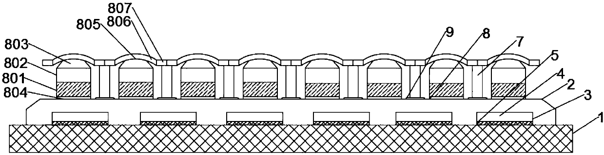
[0024] Such as Figure 1 to Figure 4 As shown, the present invention provides a heat dissipation structure for the surface of a microelectronic chip, including a chip substrate 1 and a heat conduction sheet 2, the heat conduction sheet 2 is arranged on the surface of the chip substrate 1, and the inside of the heat conduction sheet 2 is provided with several A perforation 3, the interior of the perforation 3 is provided with a heat-conducting silica gel pad 4, the heat-conducting silica gel pad 4 and the chip substrate 1 are connected together through a polytetrafluoroethylene insulating layer 5, and the heat-conducting silica gel pad 4 is used to make the heat-conducting sheet 2 and the chip substrate 1 connected together. The bonding between the chip substrates 1 is tighter, avoiding gaps, improving the heat dissipation effect and protecting the chip substrates;

[0025] The interior of the polytetrafluoroethylene insulating layer 5 adopts a porous structure, and the interio...


PUM


Abstract

The invention discloses a heat dissipation structure used for the surface of a microelectronic chip. The heat dissipation structure comprises a chip substrate and a heat conducting sheet; the heat conducting sheet is arranged on the surface of the chip substrate; a plurality of through holes are formed in the heat conducting sheet; heat conducting silica gel cushions are arranged in the through holes; a plurality of wet conduction fiber pipes are arranged on the surface of the heat conducting sheet; the wet conduction fiber pipes are arranged uniformly; heat dissipation heat pipes are arrangedbetween adjacent wet conduction fiber pipes; each heat dissipation heat pipe comprises a heat absorption section, an evaporation section and a condensation section which are connected in sequence from the bottom up; the heat absorption section and the heat conducting sheet are fixedly connected together; the top end of the condensation section is connected with an aluminum sheet; the aluminum sheet comprises an arc-shaped section and a horizontal section; and the arc-shaped section is higher than the horizontal section. By virtue of combination of a direct heat conduction mode and an indirectheat dissipation mode entirely, the microelectronic chip can be subjected to high heat dissipation, so that the temperature of the microelectronic chip can be lowered effectively, the chip can be protected effectively, the service life can be prolonged, and the heat dissipation structure is worthy of popularization.

Description

technical field [0001] The invention relates to the technical field of microelectronics, in particular to a heat dissipation structure used on the surface of a microelectronic chip. Background technique [0002] Microelectronics technology is a new technology developed along with integrated circuits, especially VLSIs. The theoretical basis of its development is modern physics established from the end of the 19th century to the 1930s. Microelectronics technology includes a series of specialized technologies such as system circuit design, device physics, process technology, material preparation, automatic testing, packaging, and assembly. , Microelectronics technology is the sum of various process technologies in microelectronics. With the development of microelectronics technology, microelectronic chips are becoming more and more popular, but because microelectronic chips need to work for a long time, they will generate a certain amount of heat. If the heat cannot be dissipa...

Claims


Application Information

Patent Timeline
IPC IPC(8): H01L23/367H01L23/373H01L23/427H01L23/467
CPCH01L23/367H01L23/3737H01L23/427H01L23/467
Inventor 强俊阜稳稳孔智慧陈恩涛盛周璇彭壮李远洋
Owner ANHUI UNIVERSITY OF TECHNOLOGY AND SCIENCE
Why Eureka
Try Eureka