Semiconductor device and preparation method thereof

A semiconductor and conductor technology, applied in the field of semiconductor devices forming 3D NAND flash memory and its preparation, can solve problems such as ion diffusion, temperature limitation, and affecting product performance

Active Publication Date: 2018-02-02
YANGTZE MEMORY TECH CO LTD
View PDF10 Cites 104 Cited by
  • Summary
  • Abstract
  • Description
  • Claims
  • Application Information

AI Technical Summary

Problems solved by technology

[0006] However, the disadvantage of the above-mentioned patented technology is that the above-mentioned vertical channel memory device is fabricated sequentially on only one Si substrate layer, so the temperature

Method used


Image

  • Semiconductor device and preparation method thereof
  • Semiconductor device and preparation method thereof
  • Semiconductor device and preparation method thereof

Examples


Embodiment Construction

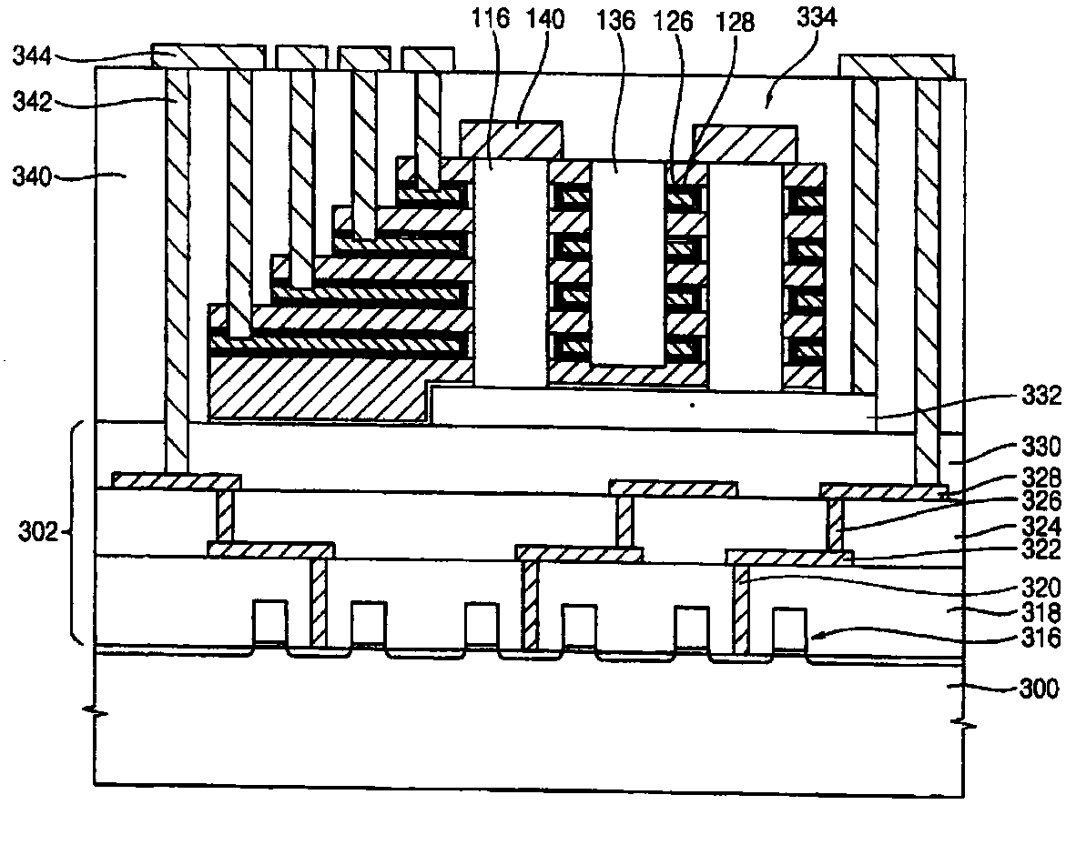
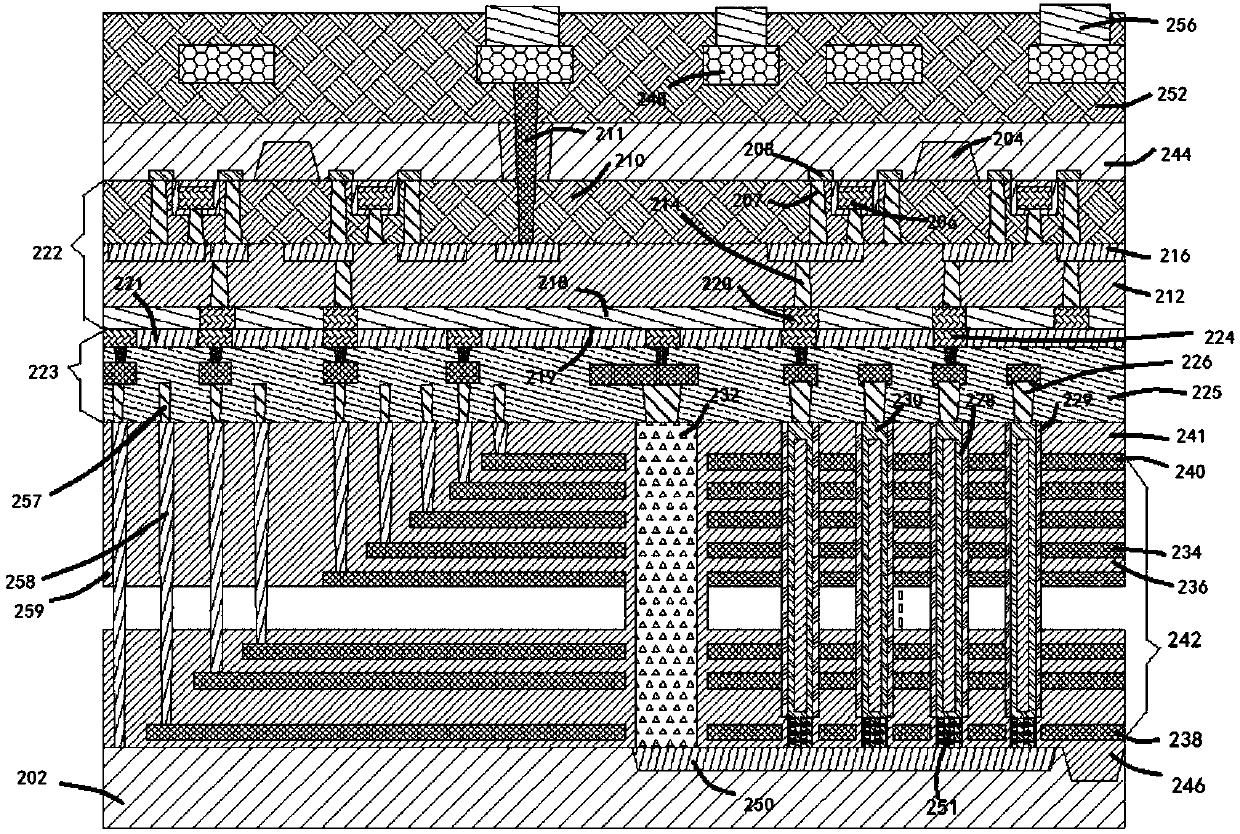
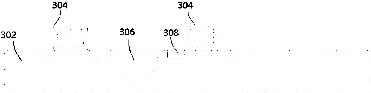
[0056]Embodiments of the invention will be described more fully hereinafter with reference to the accompanying drawings, in which preferred embodiments of the invention are shown. However, this invention may be embodied in various ways and should not be construed as limited to only the embodiments set forth herein. Like reference numerals refer to like elements throughout the specification.

[0057] It will be understood that, although the terms first, second etc. may be used herein to describe various elements, these elements should not be limited by these terms. These terms are used to distinguish one element from another. For example, a first element could be termed a second element, and, similarly, a second element could be termed a first element, without departing from the scope of the present invention. As used herein, the term "and / or" includes any and all combinations of one or more of the associated listed items.

[0058] It will be understood that when an element ...


PUM


Abstract

The invention discloses a semiconductor device and a preparation method thereof. The semiconductor device sequentially comprises a silicon substrate, one or more NAND strings formed at the upper partof the silicon substrate, one or more peripheral devices formed at the upper parts of the NAND strings, a monocrystal silicon layer formed at the upper parts of the one or more peripheral devices, andone or more first interconnection layers formed between the one or more peripheral devices and between the one or more NAND strings from bottom to top, wherein the peripheral devices are bonded withan array device through a bonding interface. The preparation process that two devices are affected by each other when prepared can be avoided through separating preparation of the array device and theperipheral devices, so that the problem of temperature limitation of preparation of the front layer to preparation of the back layer in the prior art is solved, thereby obtaining good performance ofthe peripheral devices. In addition, the peripheral devices are superposed on the array device, thereby achieving high device density.

Description

technical field [0001] The invention relates to a semiconductor device and a preparation method thereof, in particular to a semiconductor device forming a 3D NAND flash memory and a preparation method thereof. Background technique [0002] With the continued emphasis on highly integrated electronics, there is a continuing need for semiconductor memory devices that operate at higher speeds and lower power and have increased device densities. To this end, devices with smaller dimensions and multilayer devices with transistor cells arranged in horizontal and vertical arrays have been developed. 3D NAND is an emerging type of flash memory developed by the industry. It solves the limitations of 2D or planar NAND flash memory by stacking memory particles together. [0003] The planar structure of NAND flash memory is approaching its actual expansion limit, which brings severe challenges to the semiconductor memory industry. The new 3D NAND technology stacks multiple layers of da...

Claims


Application Information

Patent Timeline
IPC IPC(8): H01L27/11578H01L27/1157H01L27/11551H01L27/11524
CPCH10B41/20H10B41/35H10B43/20H10B43/35H01L27/0688H10B43/50H10B43/40H10B43/27
Inventor 朱继锋吕震宇陈俊胡禺石陶谦杨士宁杨伟毅
Owner YANGTZE MEMORY TECH CO LTD
Why Eureka
Try Eureka