
Manufacturing method of grid insulation layer

A gate insulating layer and radio frequency power technology, which is applied in semiconductor/solid-state device manufacturing, electrical components, semiconductor devices, etc., can solve the problems of removing trapped charges, difficulty, and charge capture on the surface of the gate insulating layer, achieving high reliability performance, high yield

Inactive Publication Date: 2018-02-06
WUHAN XINXIN SEMICON MFG CO LTD
View PDF3 Cites 0 Cited by
  • Summary
  • Abstract
  • Description
  • Claims
  • Application Information

AI Technical Summary

Problems solved by technology

[0003] GOI (Gate Oxide Integrity, referred to as GOI) is an important criterion for measuring the failure of MOS devices. One of the reasons for the GOI problem in the prior art is the appearance of the surface of the gate insulating layer caused by the process of the gate insulating layer. In the case of charge trapping, it is difficult to remove the trapped charge through subsequent processes, and the GOI problem cannot be avoided

Method used


Image

  • Manufacturing method of grid insulation layer
  • Manufacturing method of grid insulation layer

Examples


preparation example Construction

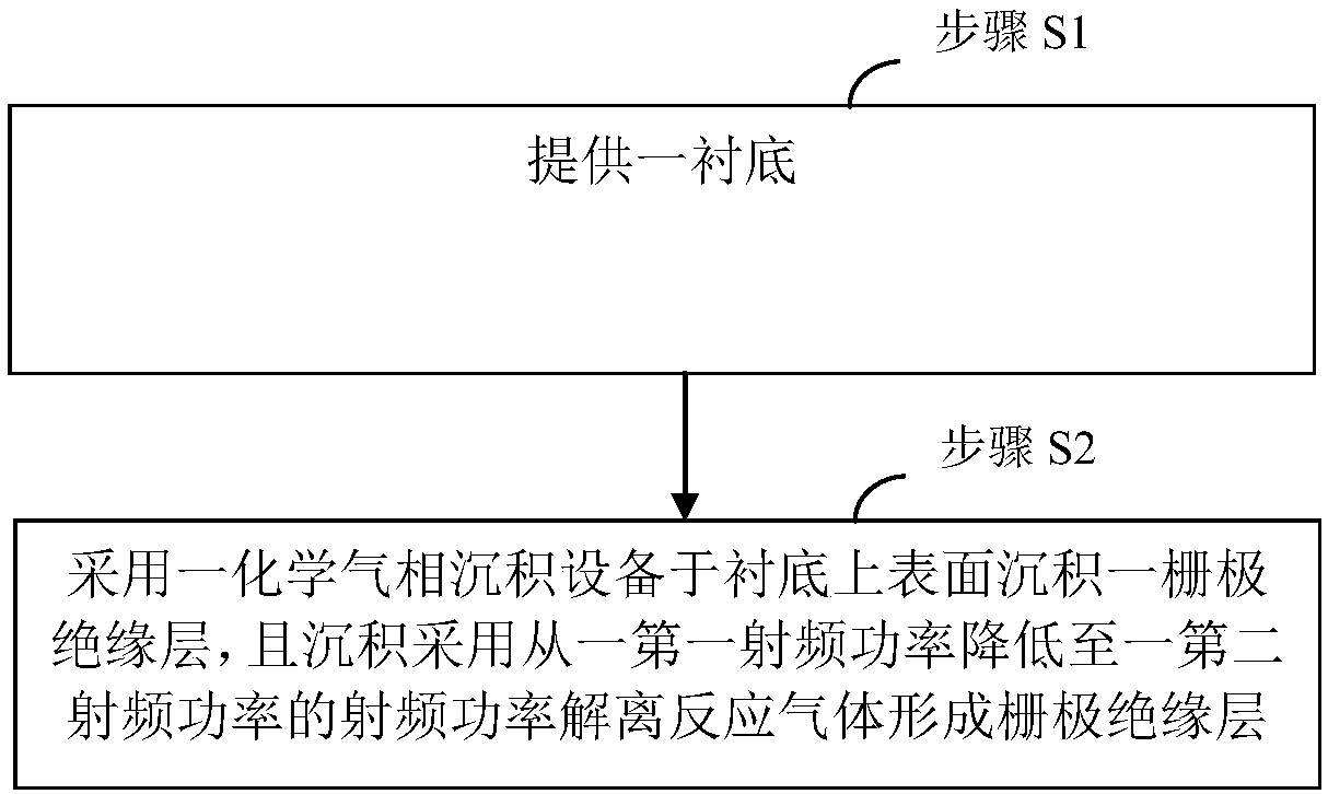
[0021] In a preferred embodiment, as figure 1 As shown, a method for preparing a gate insulating layer is proposed, which may include:

[0022] Step S1, providing a substrate;

[0023] Step S2, using a chemical vapor deposition apparatus to deposit a gate insulating layer on the upper surface of the substrate, and depositing the gate insulating layer by using a radio frequency power reduced from a first radio frequency power to a second radio frequency power to dissociate a reactive gas;

[0024] Wherein, the second radio frequency power is 0-50W (W).

[0025] In the above technical solution, the second radio frequency power should be smaller than the first radio frequency power; the chemical vapor deposition equipment initially uses a higher first radio frequency power to dissociate the reaction gas to ensure the dissociation efficiency, and then gradually reduces to the second radio frequency power. The second RF power range is 0-50W, so there is no problem of charge trapp...


PUM


Abstract

The invention relates to the technical field of a semiconductor and particularly relates to a manufacturing method of a grid insulation layer. The method comprises steps that step S1, a substrate is provided; and step S2, chemical vapor deposition equipment is employed to deposit a grid insulation layer on an upper surface of the substrate, a radio frequency power reducing from a first radio frequency power to a second radio frequency power is employed to dissociate a reactant gas to form the grid insulation layer for deposition, and the second radio frequency power is in a range of 0-50W. Themethod is advantaged in that a problem of charge capture generated on the grid insulation layer can be avoided, and products are facilitated to have the high yield and high reliability.

Description

technical field [0001] The invention relates to the technical field of semiconductors, and in particular, to a method for preparing a gate insulating layer. Background technique [0002] MOSFET (Metal-Oxide-Semiconductor Field-Effect Transistor Metal-Oxide Semiconductor Field Effect Transistor, MOSFET for short) is a field effect transistor that can be widely used in analog circuits and digital circuits. The preparation of MOSFET generally requires preparation of its gate structure, and the performance of the gate structure also directly affects the performance of the MOSFET device. [0003] GOI (Gate Oxide Integrity, GOI for short) is an important criterion for measuring the failure of MOS devices. One of the reasons for the GOI problem in the prior art is the appearance of the surface of the gate insulating layer caused by the process of the gate insulating layer. In the case of charge trapping, and it is difficult to remove the trapped charge through subsequent processes...

Claims


Application Information

Patent Timeline
IPC IPC(8): H01L21/28H01L21/285
CPCH01L21/285H01L21/28158
Inventor 李想刘超潘冬
Owner WUHAN XINXIN SEMICON MFG CO LTD
Features
  • Generate Ideas
  • Intellectual Property
  • Life Sciences
  • Materials
  • Tech Scout
  • Unparalleled Data Quality
  • Higher Quality Content
  • 60% Fewer Hallucinations
Learn More