Infrared touch module and touch display device

A touch display device, infrared touch technology, applied in instruments, semiconductor devices, computing, etc., can solve the problems of inability to realize multi-touch, and the thickness of the infrared touch screen is large, achieve strong anti-interference ability, reduce thickness, overcome Thicker effect

Inactive Publication Date: 2018-02-09
BOE TECH GRP CO LTD +1
View PDF4 Cites 7 Cited by
  • Summary
  • Abstract
  • Description
  • Claims
  • Application Information

AI Technical Summary

Problems solved by technology

[0004] The technical problem to be solved by the embodiments of the present invention is to provide an infrared touch module and a touch display device to overcome the defects that the existing infrared touch screens are relatively thick and cannot realize multi-touch

Method used


Image

  • Infrared touch module and touch display device
  • Infrared touch module and touch display device
  • Infrared touch module and touch display device

Examples


no. 1 example

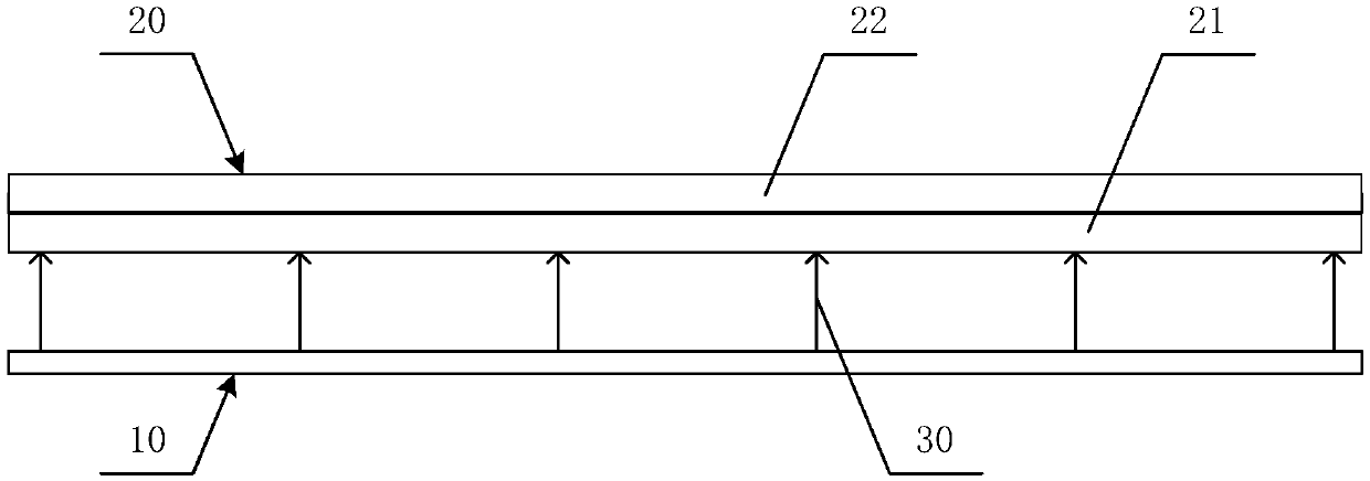
[0048] image 3 It is a schematic structural diagram of the first embodiment of the infrared touch module of the present invention, Figure 4 for image 3 Floor plan of the structure. The infrared touch module of this embodiment can be used as an independent infrared touch panel. like image 3 and 4 As shown, the main structure of the infrared touch module of this embodiment includes an infrared emitting unit 10 and a touch structural unit 20 of a layered structure, the infrared emitting unit 10 and the touch structural unit 20 are arranged oppositely, and the infrared emitting unit 10 is used for emitting Infrared light 30, the touch structure unit 20 is used to determine the touch position by changing the transmittance of infrared light when being touched. The touch structure unit 20 of this embodiment includes an interference filter layer 21, an infrared sensing layer 22, and a touch sensing layer 23. The interference filter layer 21 is arranged opposite to the infrare...

no. 2 example

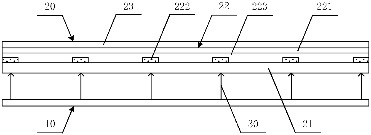
[0053] Figure 5 It is a schematic structural diagram of the second embodiment of the infrared touch module of the present invention. like Figure 5 As shown, the main structure of the infrared touch module of this embodiment is basically the same as that of the aforementioned first embodiment, the difference is that the interference filter layer 21 of this embodiment adopts an infrared short-wave interference filter film, which only transmits infrared light. The infrared short-wave interference filter film may include a plurality of strip structures, and the plurality of strip structures are arranged in parallel and at intervals. When combined with the display panel to form a touch display device, the position of each strip structure corresponds to the opaque area of ​​the display panel, that is, the interference filter layer 21 of this embodiment only covers the opaque area of ​​the display panel. In this embodiment, by arranging the interference filter layer in a striped ...

no. 3 example

[0055] Figure 6 It is a schematic structural diagram of the third embodiment of the infrared touch module of the present invention. The infrared touch module of this embodiment is a touch display device combined with a liquid crystal display panel (Liquid Crystal Display, LCD) to form an ON-Cell structure. like Figure 6 As shown, the touch display device of this embodiment includes an LCD panel and a touch structure unit disposed on the light-emitting surface of the LCD panel. The main structure of the LCD panel includes a backlight 1, an array (Thin Film Transistor, TFT) substrate 2 and a color filter (ColorFilter, CF) substrate 3, the array substrate 2 and the color filter substrate 3 are boxed and the liquid crystal (LC, Liquid Crystal) The layer 4 is arranged between the two substrates, and the backlight source 1 is arranged on one side of the array substrate 2 . The touch structure unit 20 of this embodiment includes an interference filter layer 21, an infrared sensi...


PUM


Abstract

The embodiment of the invention provides an infrared touch module and a touch display device. The infrared touch module comprises an infrared emitting unit and a touch structure unit of a layered structure, wherein the infrared emitting unit and the touch structure unit are arranged oppositely, the infrared emitting unit is used for emitting infrared rays, and the touch structure unit is used fordetermining a touch position by changing the transmittance of the infrared rays in case of touch. By the adoption of the layered structure, the thickness of the infrared touch module is effectively lowered, thinning is realized, and the infrared touch module and a display panel can form an ON-Cell or IN-Cell structure. Due to the fact that the infrared touch module determines the touch position bychanging the transmittance of the infrared rays at the touch position, multipoint touch can be realized. The embodiment effectively overcomes the defects that an existing infrared touch screen has large thickness and cannot realize multipoint touch.

Description

technical field [0001] The invention relates to the field of touch technology, in particular to an infrared touch module and a touch display device. Background technique [0002] Touch technology is an important link in the process of human-computer interaction, and display devices such as smart phones and tablet computers all need the support of touch technology. Existing touch technologies mainly include capacitive, resistive, ultrasonic and infrared. Among them, since both capacitive and resistive touch technologies have their best use environments, in abnormal environments, such as strong electromagnetic interference, the use effect of these two touch technologies will be affected, resulting in misjudgment . In contrast, the infrared touch technology has higher stability, not only has a strong ability to resist external electromagnetic wave interference, but also has a long service life, so the infrared touch technology is gradually favored by people. [0003] At pres...

Claims


Application Information

Patent Timeline
Patent Type & Authority Applications(China)
IPC IPC(8): G06F3/042G06F3/041
CPCG06F3/0412G06F3/042G06F2203/04103G02B5/281G02B26/007G02F1/13338G02F2203/11G06F3/0421G02F1/133617H10K59/40
Inventor 倪欢李媛
Owner BOE TECH GRP CO LTD
Why Eureka
Try Eureka