OLED display panel and manufacture method thereof

A technology for a display panel and a manufacturing method, which is applied in the manufacture of semiconductor/solid-state devices, electrical components, and electrical solid-state devices, etc., can solve problems such as low aperture ratio, and achieve the effects of improving light color and enhancing light-outcoupling efficiency.

Active Publication Date: 2018-02-23
SHENZHEN CHINA STAR OPTOELECTRONICS SEMICON DISPLAY TECH CO LTD
View PDF6 Cites 7 Cited by
  • Summary
  • Abstract
  • Description
  • Claims
  • Application Information

AI Technical Summary

Problems solved by technology

Achieving large-scale display requires the use of TFT drive technology, while traditional bottom-emitting OLEDs (BOLEDs) use indium tin oxide (ITO) anodes on transparent substrates as the light-emitting surface. When using non-transparent silicon substrates When the bottom or amorphous silicon with low mobility or organic TFT is used as the substrate, it is easy to cause the problem of low aperture ratio

Method used


Image

  • OLED display panel and manufacture method thereof
  • OLED display panel and manufacture method thereof
  • OLED display panel and manufacture method thereof

Examples


Embodiment Construction

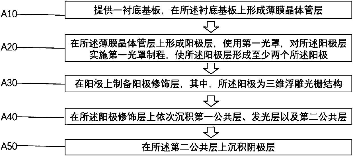
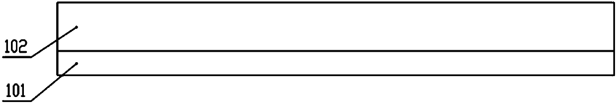
[0039] The following descriptions of the various embodiments refer to the accompanying drawings to illustrate specific embodiments in which the invention may be practiced. The directional terms mentioned in the present invention, such as [top], [bottom], [front], [back], [left], [right], [inside], [outside], [side], etc., are only for reference The orientation of the attached schema. Therefore, the directional terms used are used to illustrate and understand the present invention, but not to limit the present invention. In the figures, structurally similar elements are denoted by the same reference numerals.

[0040] The present invention is aimed at the existing OLED display panel, without preparing the structure of the total reflection anode and the semitransparent cathode in the OLED preparation process to realize the top emission of the OLED device, but introducing a The novel structure achieves the effect of improving the light color emitted by the OLED device and enhan...


PUM


Abstract

The invention provides an OLED display panel and a manufacture method thereof. The OLED display panel comprises a thin film transistor layer, an anode layer, an anode modification layer, a first public layer, a light emitting layer, a second public layer and a cathode layer. The anode modification layer is made of an azobenzene compound, wherein the azobenzene compound contains a functional groupused for transporting holes and a functional group used for enhancing the solubility in common organic solvents. In addition, the anode modification layer is in a three-dimensional relief grating structure. The OLED display panel has the advantages that by finely adjusting the three-dimensional grating structure of the anode modification layer, the micro-cavity effect of a top-emitting OLED devicecan be adjusted to improve the light color of an OLED device; and the light-out coupling efficiency of the device is enhanced.

Description

technical field [0001] The invention relates to the technical field of flat panel display manufacturing, in particular to an OLED display panel and a manufacturing method thereof. Background technique [0002] In flat panel display technology, Organic Light-Emitting Diode (OLED) display has many advantages such as thinness, active light emission, fast response speed, large viewing angle, wide color gamut, high brightness and low power consumption, etc., and has gradually become the successor. The third generation display technology after liquid crystal display. Compared with LCD (Liquid crystal displays, liquid crystal display), OLED has the advantages of saving power, being thinner, and having a wider viewing angle, which is incomparable to LCD. At present, people have higher and higher requirements for the fineness of the display, that is, the resolution, but the production of high-quality, high-resolution OLED displays still faces many challenges. [0003] The core comp...

Claims


Application Information

Patent Timeline
IPC IPC(8): H01L51/56H01L27/32H01L51/52
CPCH10K71/00H10K59/80515H10K59/876
Inventor 张育楠
Owner SHENZHEN CHINA STAR OPTOELECTRONICS SEMICON DISPLAY TECH CO LTD
Why Eureka
Try Eureka