

A kind of germanium selenide film and preparation method thereof
A germanium selenide and thin film technology, applied in the direction of electrolytic inorganic material coating, etc., can solve the problems of scarcity of semiconductor materials and inability to respond.
- Summary
- Abstract
- Description
- Claims
- Application Information
AI Technical Summary
Problems solved by technology
Method used
Image

Examples
Embodiment 1
[0031] A kind of germanium selenide film preparation method, the steps are as follows:
[0032] 1) Weigh 10 mg of GeSe powder into 30 mL of ethanol solution, and ultrasonically vibrate for 5 min using an ultrasonic cleaner to form a dark brown suspension.
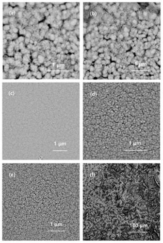
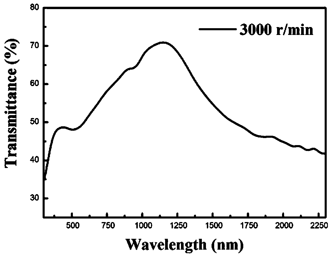
[0033] 2) Pour the suspension evenly into two centrifuge tubes, put it into a centrifuge and centrifuge for 7min, the speed of the centrifuge is 2000r / min, 3000r / min, 4000r / min, 5000r / min, 6000r / min, centrifuge Then take the supernatant in a 50mL beaker.
[0034] 3) Weigh 3 mg of iodine powder and add it to the supernatant liquid obtained by centrifugation, and then ultrasonically shake for 5 minutes to fully disperse the iodine powder particles in ethanol and positively charge the GeSe particles.
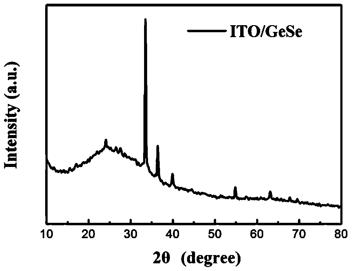
[0035] 4) Connect the ITO substrate on which the GeSe film needs to be deposited to the negative pole of the DC stabilized power supply, connect the metal titanium sheet to the positive pole of the DC stabilized power supply, a...
Embodiment 2
[0039] A method for preparing a germanium selenide thin film, the steps are as follows:
[0040] 1) Weigh 20 mg of GeSe powder into 60 mL of ethanol solution, and ultrasonically vibrate for 7 minutes using an ultrasonic cleaner to form a dark brown suspension.
[0041] 2) Pour the suspension evenly into two centrifuge tubes, put it into a centrifuge and centrifuge for 7min, the speed of the centrifuge is 2000r / min, 3000r / min, 4000r / min, 5000r / min, 6000r / min, centrifuge Then take the supernatant in a 50mL beaker.
[0042] 3) Weigh 6 mg of iodine powder and add it to the supernatant obtained by centrifugation, and then ultrasonically shake for 7 minutes to fully disperse the iodine powder particles in ethanol and positively charge the GeSe particles.
[0043] 4) Connect the ITO substrate on which the GeSe film needs to be deposited to the negative pole of the DC stabilized power supply, connect the metal titanium sheet to the positive pole of the DC stabilized power supply, and...
Embodiment 3
[0047] A method for preparing a germanium selenide thin film, the steps are as follows:
[0048] Weigh 30 mg of GeSe powder into 100 mL of ethanol solution, and ultrasonically shake for 7 min using an ultrasonic cleaner to form a dark brown suspension.
[0049] 2) Pour the suspension into two centrifuge tubes evenly, put it into a centrifuge and centrifuge for 10 minutes, the speed of the centrifuge is 2000r / min, 3000r / min, 4000r / min, 5000r / min, 6000r / min, centrifuge Then take the supernatant in a 50mL beaker.
[0050] 3) Weigh 10 mg of iodine powder and add it to the supernatant obtained by centrifugation, and then ultrasonically vibrate for 10 minutes to fully disperse the iodine powder particles in ethanol and to make the GeSe particles positively charged.
[0051] 4) Connect the ITO substrate on which the GeSe film needs to be deposited to the negative pole of the DC stabilized power supply, connect the metal titanium sheet to the positive pole of the DC stabilized power su...
PUM
 Abstract
Description
Claims
Application Information