
Patsnap Eureka
For R&D, Patsnap Eureka makes reading and utilizing patents & technical documents easy.
Patsnap Eureka AIR
Designed for self-driven R&D workflows. Generate viable solutions, solve complex R&D challenges, empower your innovation with AI.

Patsnap Eureka Materials
Designed for material experts only. Revolutionize your material R&D, from search, analyze, to developing new materials.

TechResearch
Generate reliable direction feasibility study reports for your R&D in just a few steps.

TechSeek
Discover and master advanced knowledge NOW. Basics, ideas, possibilities, all at once.

TechMind
As an expert in R&D Theories, TechMind can generates customized viable solutions instantly.

TechRisk
Analyze your overall solution with one click, know your potential R&D risks in advance.

TechMonitor
Get weekly tech updates, stay abreast of the latest tech innovations and key insights.
Monocrystalline silicon seed crystal splicing method
A monocrystalline silicon and seed crystal technology, which is applied in the field of photovoltaic solar cell manufacturing, can solve the problem of large gaps in monocrystalline silicon seed crystals
- Summary
- Abstract
- Description
- Claims
- Application Information
AI Technical Summary
Problems solved by technology
Method used
Image

Examples
Embodiment 1
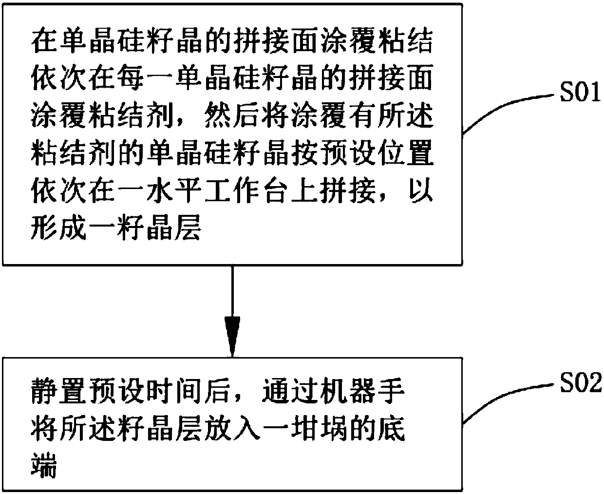
[0027] see Figure 1 to Figure 3 A method for splicing single crystal silicon seed crystals according to the first embodiment of the present invention includes step S01 and step S02.
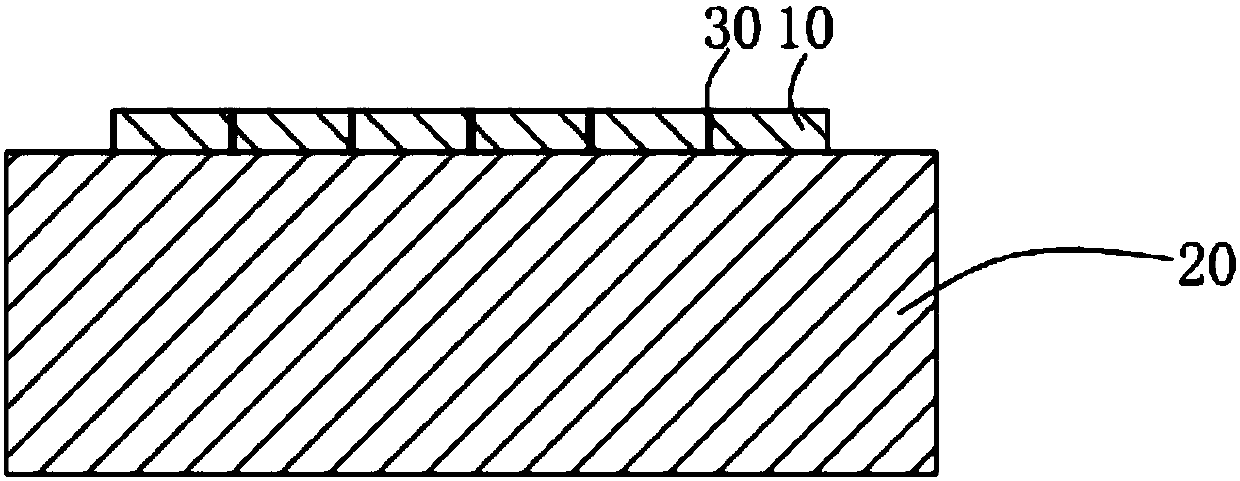
[0028] Step S01, coating the bonding agent on the splicing surface of each silicon single crystal seed crystal 10 in sequence, and then placing the single crystal silicon seed crystal 10 coated with the adhesive 30 on a surface roughness Splice on a horizontal workbench 20 smaller than 0.2 mm to form a seed layer 100 .
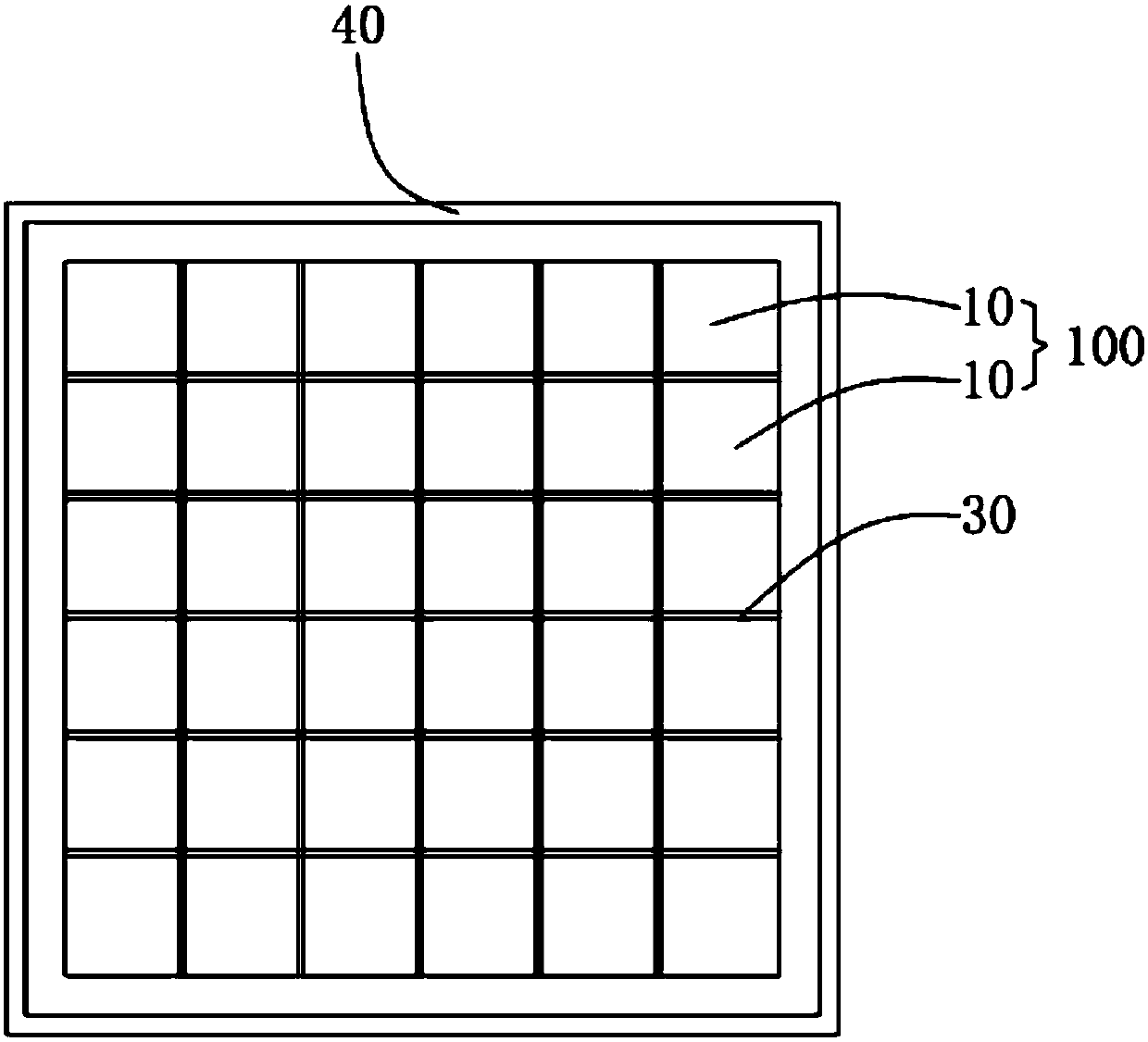
[0029] Specifically, in this embodiment, 36 single-crystal silicon seed crystals 10 are selected in advance, and the height difference between every two single-crystal silicon seed crystals is less than 1mm, and these 36 single-crystal silicon seed crystals 10 are sequentially placed Coat the bonding agent 30 on the splicing surface, and sequentially splice 36 single crystal silicon seed crystals 10 in a 6×6 manner to form a seed crystal layer 100 .
[0030] It can be understo...
Embodiment 2
[0042] A method for splicing single crystal silicon seed crystals provided by the second embodiment of the present invention includes step S11 and step S12.
[0043] Step S11, selecting 49 single crystal silicon seed crystals 10, coating the bonding agent on the splicing surface of each single crystal silicon seed crystal 10 in turn, and then coating the single crystal silicon seed crystals 10 coated with the adhesive 30 49 single crystal silicon seed crystals 10 were spliced sequentially in a 7×7 manner on a horizontal workbench 20 with a surface roughness less than 0.2 mm to form a seed crystal layer 100 .
[0044] Specifically, in this embodiment, the main components of the binder 30 include a mixture of silica sol and ceramic binder, and the mixing ratio of silica sol and ceramic binder is 1:1.
[0045] Step S12, after standing still for 3600s, put the seed crystal layer 100 into the bottom end of the crucible 40 by the robot.
Embodiment 3
[0047] A method for splicing single crystal silicon seed crystals provided by the third embodiment of the present invention includes step S21 and step S22.
[0048] Step S21, select 25 single crystal silicon seed crystals 10, apply adhesive on the splicing surface of each single crystal silicon seed crystal 10 in turn, and then place the single crystal silicon seed crystals 10 coated with the adhesive 30 25 single crystal silicon seed crystals 10 are spliced sequentially in a 5×5 manner on a horizontal workbench 20 with a surface roughness less than 0.2 mm to form a seed crystal layer 100 .
[0049] Specifically, in this embodiment, the main components of the binder 30 include a mixture of silica sol and ceramic binder, and the mixing ratio of silica sol and ceramic binder is 2:1.
[0050] Step S22, after standing still for 1800s, put the seed crystal layer 100 into the bottom end of the crucible 40 by robot.
[0051] Combining with Example 1, Example 2, and Example 3, it c...
PUM
 Abstract
Description
Claims
Application Information
 - R&D Engineer
- R&D Manager
- IP Professional
- Industry Leading Data Capabilities
- Powerful AI technology
- Patent DNA Extraction
Browse by: Latest US Patents, China's latest patents, Technical Efficacy Thesaurus, Application Domain, Technology Topic, Popular Technical Reports.
© 2024 PatSnap. All rights reserved.Legal|Privacy policy|Modern Slavery Act Transparency Statement|Sitemap|About US| Contact US: help@patsnap.com