Fan-shaped antenna packaging structure and preparation method thereof

A technology of packaging structure and antenna structure, which is applied in the direction of antenna support/mounting device, antenna, loop antenna, etc., can solve the problem of enlarging the area of ​​the packaging structure, achieve the effect of small line width, increase gain, and ensure stability

Pending Publication Date: 2018-02-27
SJ SEMICON JIANGYIN CORP
View PDF13 Cites 9 Cited by
  • Summary
  • Abstract
  • Description
  • Claims
  • Application Information

AI Technical Summary

Problems solved by technology

[0006] In view of the above-mentioned shortcomings of the prior art, the object of the present invention is to provide a fan-out antenna packaging structure and its preparation method, which is used to solve the problem that the size and area of ​​the antenna must be sufficient to ensure the antenna gain when the existing radio frequency chip is in use. Large, which leads to the problem that the area of ​​the PCB board and the area of ​​the entire package structure become larger

Method used


Image

  • Fan-shaped antenna packaging structure and preparation method thereof
  • Fan-shaped antenna packaging structure and preparation method thereof
  • Fan-shaped antenna packaging structure and preparation method thereof

Examples


Embodiment 1

[0077] see figure 1 , the present invention provides a method for preparing a fan-out antenna package structure, the method for preparing a fan-out antenna package structure includes the following steps:

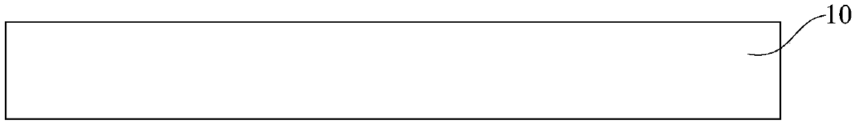
[0078] 1) providing a carrier, and forming a release layer on the upper surface of the carrier;

[0079] 2) Provide a semiconductor chip, and install the semiconductor chip on the surface of the peeling layer facing down;

[0080] 3) forming a metal connection column on the surface of the peeling layer;

[0081] 4) forming a plastic sealing material layer on the surface of the peeling layer, the plastic sealing material layer fills the gap between the semiconductor chip and the metal connecting column, and plastic seals the semiconductor chip and the metal connecting column; The molding material layer includes opposite first surfaces and second surfaces, the second surface of the molding material layer is in contact with the release layer, and the first surface of the mold...

Embodiment 2

[0145] read on Figure 13 and Figure 14, the present embodiment also provides a fan-out antenna package structure, the fan-out antenna package structure includes: a semiconductor chip 12; a plastic packaging material layer 14, the plastic packaging material layer 14 includes an opposite first surface and a second surface , the plastic packaging material layer 14 is plastic-sealed on the periphery of the semiconductor chip 12, and exposes the front side of the semiconductor chip 12; the metal connection column 13, the metal connection column 13 is located in the plastic packaging material layer 14, and up and down Penetrating through the plastic packaging material layer 14; the antenna structure 16, the antenna structure 16 is located on the first surface of the plastic packaging material layer 14, and is electrically connected to the metal connecting column 13; the rewiring layer 15, the rewiring Layer 15 is located on the second surface of the plastic packaging material lay...


PUM


Abstract

The invention provides a fan-shaped antenna packaging structure and a preparation method thereof. The structure comprises a semiconductor chip, a plastic sealing material layer, metal connecting columns, an antenna structure, a rewiring layer and solder bumps; the plastic sealing material layer comprises a first surface and a second surface which are opposite to each other and is arranged on the periphery of the semiconductor chip through plastic sealing; the metal connecting columns are located in the plastic sealing material layer and penetrate through the plastic sealing material layer in an up-down mode; the antenna structure is located on the first surface of the plastic-sealing material layer and electrically connected with the metal connecting columns; the rewiring layer is locatedon the second surface of the plastic sealing material layer and electrically connected with the semiconductor chip and the metal connecting columns; the solder bumps are located on the surface, away from the plastic sealing material layer, of the rewiring layer and electrically connected with the rewiring layer. By means of the packaging structure, the space area can be greatly saved, antennas large in area length can be formed in a small region area, the antenna gain is greatly improved, the wire width of the metal antennas in the antenna structure can be very small, and the density of the metal antennas in the antenna structure can be greatly increased.

Description

technical field [0001] The invention relates to the technical field of semiconductor packaging, in particular to a fan-out antenna packaging structure and a preparation method thereof. Background technique [0002] Lower cost, more reliable, faster and higher density circuits are the goals pursued by integrated circuit packaging. In the future, integrated circuit packaging will increase the integration density of various electronic components by continuously reducing the minimum feature size. Currently, advanced packaging methods include: Wafer Level Chip Scale Packaging (WLCSP), Fan-Out Wafer Level Package (FOWLP), Flip Chip, Package on Package (Package on Package, POP) and so on. [0003] Fan-out wafer-level packaging is an embedded chip packaging method for wafer-level processing. It is currently one of the advanced packaging methods with more input / output ports (I / O) and better integration flexibility. Compared with conventional wafer-level packaging, fan-out wafer-le...

Claims


Application Information

Patent Timeline
Patent Type & Authority Applications(China)
IPC IPC(8): H01Q1/22H01Q7/00H01L23/66
CPCH01L23/66H01Q1/2283H01Q7/00H01L2223/6677H01L2224/04105H01L2224/12105H01L2224/18
Inventor 陈彦亨林正忠吴政达林章申何志宏
Owner SJ SEMICON JIANGYIN CORP
Why Eureka
Try Eureka