LDMOS (Lateral Diffusion MOS) structure

A transistor and isolation structure technology, applied in the field of LDMOS transistor structure, can solve problems such as avalanche breakdown of LDMOS structure, achieve the effects of reducing impact ionization, high breakdown voltage and saturation leakage current, and controlling production costs

Active Publication Date: 2018-03-09
SEMICONDUCTOR MANUFACTURING INTERNATIONAL (BEIJING) CORP +1
View PDF3 Cites 4 Cited by
  • Summary
  • Abstract
  • Description
  • Claims
  • Application Information

AI Technical Summary

Problems solved by technology

[0006] In view of the above-mentioned shortcomings of the prior art, the purpose of the present invention is to provide an L-DMOS transistor structure for solving the problem that the LDMOS structure is prone to avalanche breakdown in the prior art

Method used


Image

  • LDMOS (Lateral Diffusion MOS) structure
  • LDMOS (Lateral Diffusion MOS) structure
  • LDMOS (Lateral Diffusion MOS) structure

Examples


Embodiment 1

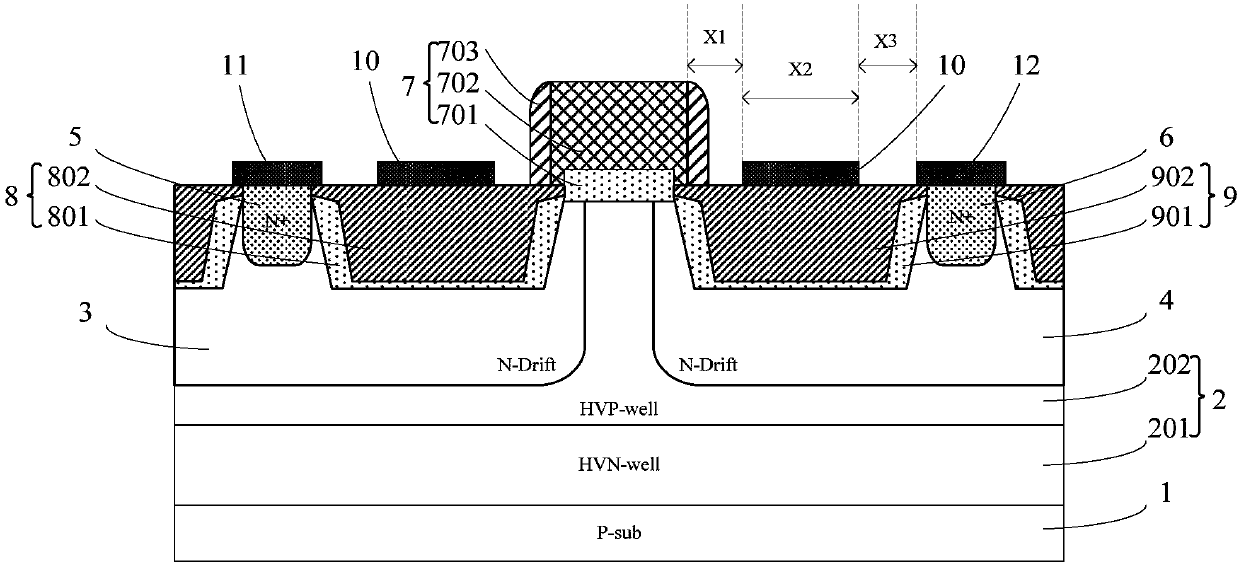
[0053] The present invention provides a LDMOS transistor structure, please refer to figure 1 , Shown as a schematic cross-sectional structure diagram of the LDMOS transistor structure, including:

[0054] Semiconductor substrate 1;

[0055] A first drift region 3 and a second drift region 4 located in the semiconductor substrate 1 and arranged separately;

[0056] A source 5 located in the first drift region 3 and a drain 6 located in the second drift region 4;

[0057] A gate structure 7 located on the semiconductor substrate 1 and contacting the first drift region 3 and the second drift region 4 on both sides;

[0058] A first isolation structure 8 located in the first drift region 3 and separating the source electrode 5 from the gate structure 7; located in the second drift region 4 and separating the drain electrode 6 from the gate structure 7 The second isolation structure 9 isolated by the gate structure 7; wherein:

[0059] A floating field plate 10 is provided on the first isol...

Embodiment 2

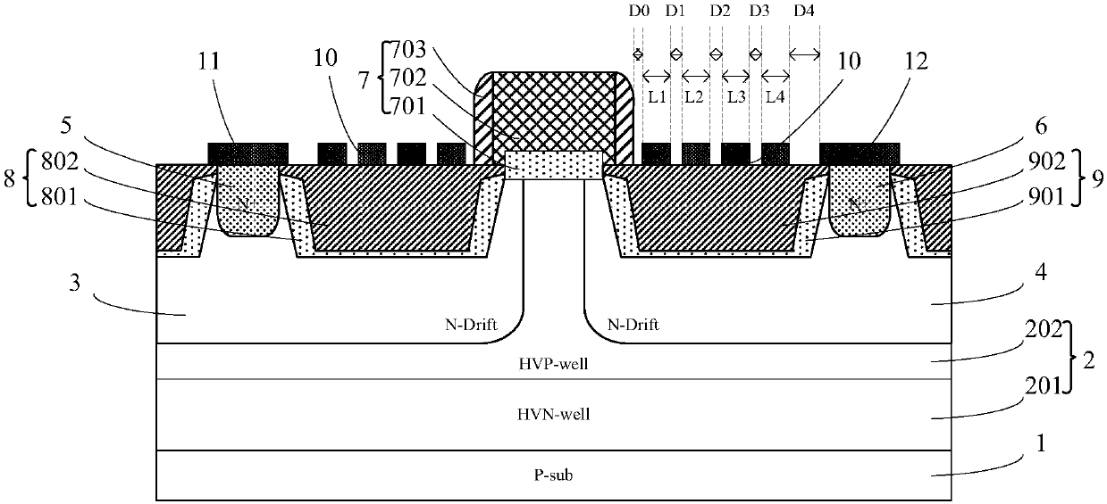
[0077] The difference between this embodiment and the first embodiment is that in the first embodiment, the first isolation structure 8 and the second isolation structure 9 are each provided with a floating field plate 10. In this embodiment, the first isolation structure and the second isolation structure are each provided with a plurality of discrete floating field plates.

[0078] See figure 2 , Showing a schematic cross-sectional structure diagram of the LDMOS transistor structure in this embodiment, including:

[0079] Semiconductor substrate 1;

[0080] A first drift region 3 and a second drift region 4 located in the semiconductor substrate 1 and arranged separately;

[0081] A source 5 located in the first drift region 3 and a drain 6 located in the second drift region 4;

[0082] A gate structure 7 located on the semiconductor substrate 1 and contacting the first drift region 3 and the second drift region 4 on both sides;

[0083] A first isolation structure 8 located in the f...


PUM


Abstract

The invention provides a LDMOS (Lateral Diffusion MOS) structure. The LDMOS structure comprises a semiconductor substrate, a first drift area and a second drift area which are located in the semiconductor substrate and are arranged separately, a source which is located in the first drift area, a drain which is located in the second drift area, a gate structure which is located on the semiconductorsubstrate and whose two sides are contacted with the first drift area and the second drift area respectively, a first isolation structure which is located in the first drift area and isolates the source and the gate structure, and a second isolation structure which is located in the second drift area and isolates the drain and the gate structure, wherein both the first isolation structure and thesecond isolation structure are provided with floating field plates. One or more floating field plates is arranged on the isolation structures between the source-gate and the drain-gate, the area of adepleted area can be increased, collision ionization can be reduced, higher breakdown voltage and saturation leakage current Idsat can thus be acquired, and the gate-drain capacitance Cgd and the gate-source capacitance Cgs of the device are not deteriorated.

Description

Technical field [0001] The invention belongs to the field of semiconductor integrated circuits and relates to an LDMOS transistor structure. Background technique [0002] Liquid Crystal Display (LCD) is a display device with good development prospects. The more commonly used LCD devices are STN (Super Twisted Type) and TFT (Thin Film Transistor Type). The process platform based on SPOCULL (Smic polycontact ultra low leakage) technology is aimed at the LCD driver market and has a good application prospect. The characteristic of SPOCULL technology is that the polysilicon connection layer covers the active area instead of the traditional metal connection, which can achieve a smaller chip area. [0003] Lateral Diffusion MOS (LDMOS), due to its high breakdown voltage and compatibility with CMOS technology, is widely used in power devices. Compared with traditional MOS transistors, LDMOS devices have at least one isolation structure between the drain region and the gate. When the LDM...

Claims


Application Information

Patent Timeline
Patent Type & Authority Applications(China)
IPC IPC(8): H01L29/78H01L29/40
CPCH01L29/404H01L29/7816
Inventor 王伟江宇雷陈玉华魏琰
Owner SEMICONDUCTOR MANUFACTURING INTERNATIONAL (BEIJING) CORP
Why Eureka
Try Eureka