Standard cell library layout design method for reducing WPE effect

A standard cell library, standard cell technology, used in computing, special data processing applications, instruments, etc., can solve problems such as increased threshold voltage, reduced circuit turn-on speed, and reduced circuit operating frequency, and achieve higher threshold voltage and circuit speed. boosted effect

Active Publication Date: 2018-03-13
SHANGHAI HUALI MICROELECTRONICS CORP
View PDF6 Cites 1 Cited by
  • Summary
  • Abstract
  • Description
  • Claims
  • Application Information

AI Technical Summary

Problems solved by technology

The disadvantage is that, in the case of a fixed area, the source and drain regions of the PMOS transistor are relatively close to the N well, and the source and drain regions of the NMOS transistor are relatively close to the P sub, so PMOS and NMOS are affected by The WPE effect has a significant impact, and the threshold voltage increases, resulting in a decrease in the opening speed of the circuit, resulting in a decrease in the operating frequency of the circuit

Method used


Image

  • Standard cell library layout design method for reducing WPE effect
  • Standard cell library layout design method for reducing WPE effect
  • Standard cell library layout design method for reducing WPE effect

Examples


Embodiment Construction

[0031] The following will clearly and completely describe the technical solutions in the embodiments of the present invention with reference to the accompanying drawings in the embodiments of the present invention. Obviously, the described embodiments are only some, not all, embodiments of the present invention. Based on the embodiments of the present invention, all other embodiments obtained by persons of ordinary skill in the art without creative efforts fall within the protection scope of the present invention.

[0032] It should be noted that, in the case of no conflict, the embodiments of the present invention and the features in the embodiments can be combined with each other.

[0033] The present invention will be further described below in conjunction with the accompanying drawings and specific embodiments, but not as a limitation of the present invention.

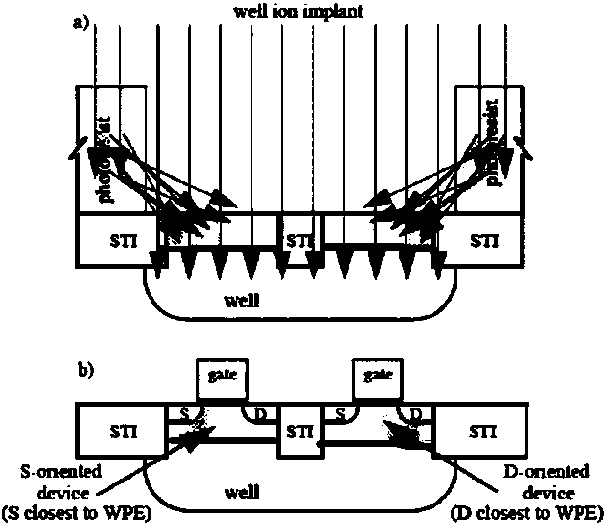
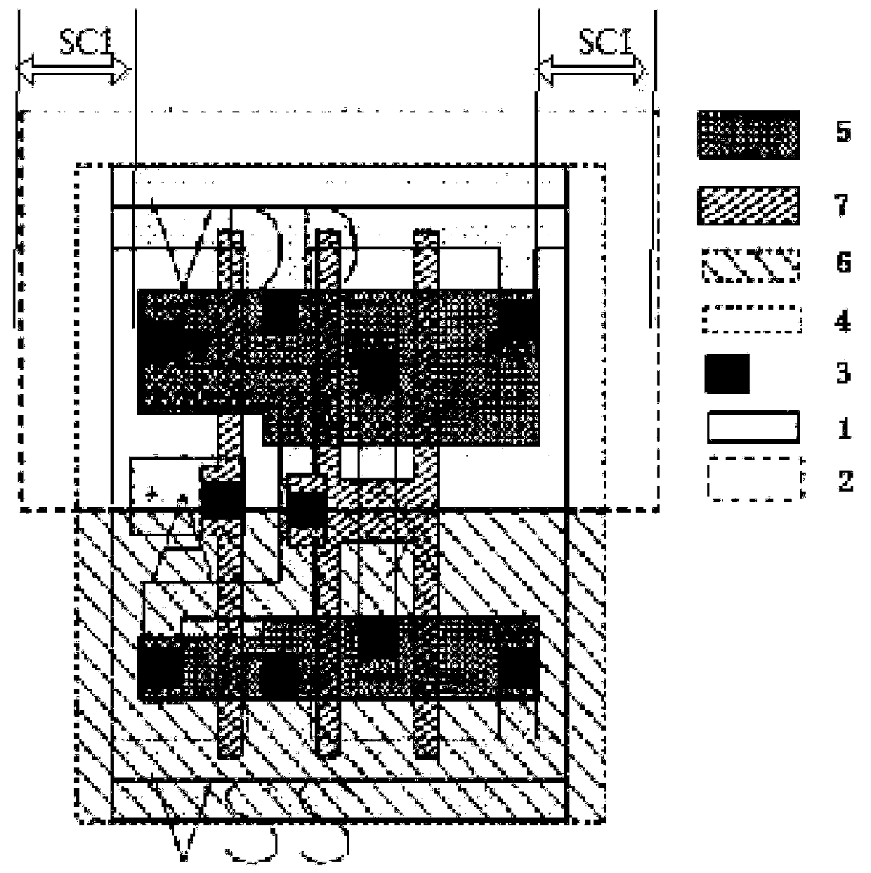
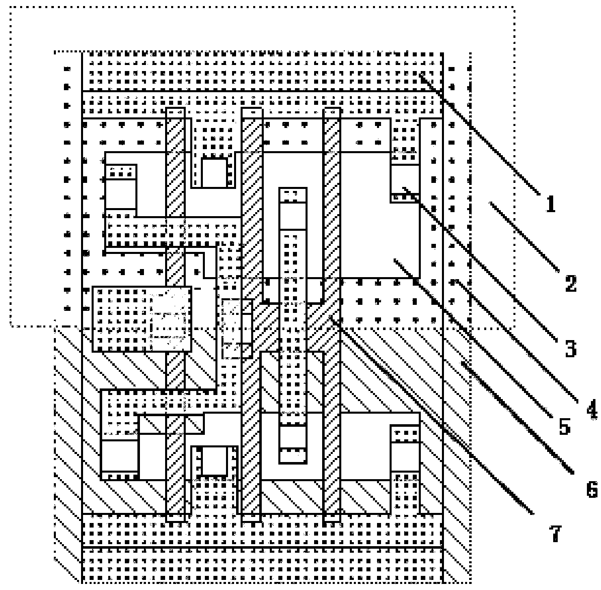
[0034] In a preferred embodiment, as Figure 3-6 As shown, a standard cell library layout design method to redu...


PUM


Abstract

The invention provides a standard cell library layout design scheme for reducing a WPE effect. The standard cell library layout design scheme is applied to the field of semiconductor manufacturing, and a standard cell library layout design method comprises the following steps that basic design parameters of standard cell layout are determined; according to a standard cell schematic diagram and thebasic design parameters, basic layout of a standard cell is formed; according to the basic layout of the standard cell, the maximum distance (SC_sum) of the PMOS AA active area of the single standardcell to a well N is calculated; according to the maximum distance (SC_sum), the best distance value from the source / drain end of a PMOS to the well N is calculated; according to the best distance value, the basic layout is adjusted. The standard cell library layout design method has the advantages that the influence of the WPE effect on the standard cell is reduced while the single standard celllayout and area fixation are achieved, threshold voltage is improved, and the circuit speed is improved by 5% or above.

Description

technical field [0001] The invention relates to the field of semiconductor manufacturing, in particular to a standard cell library layout design method for reducing the WPE effect. Background technique [0002] Such as figure 1 As shown, the Well Proximity Effect (WPE: Well Proximity Effect) means that during the ion implantation process, atoms diffuse from the edge of the mask, and the surface of the silicon wafer near the edge of the well becomes dense, and the concentration will increase with the distance from the mask. The distance of the edge of the well is different, resulting in uneven doping concentration of the entire well, and the threshold voltage of the MOS tube is also different, which affects the circuit performance. [0003] figure 2 For a typical standard cell, the layout of the buffer (Buffer) is composed of PMOS and NMOS. The disadvantage is that, in the case of a fixed area, the source and drain regions of the PMOS transistor are relatively close to th...

Claims


Application Information

Patent Timeline
Patent Type & Authority Applications(China)
IPC IPC(8): G06F17/50
CPCG06F30/392G06F30/398
Inventor 阳媛高唯欢胡晓明
Owner SHANGHAI HUALI MICROELECTRONICS CORP
Why Eureka
Try Eureka