
Aluminum gasket etching method

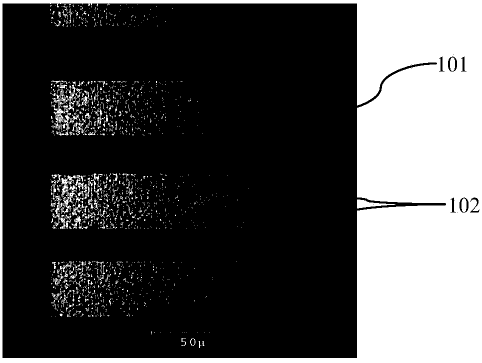
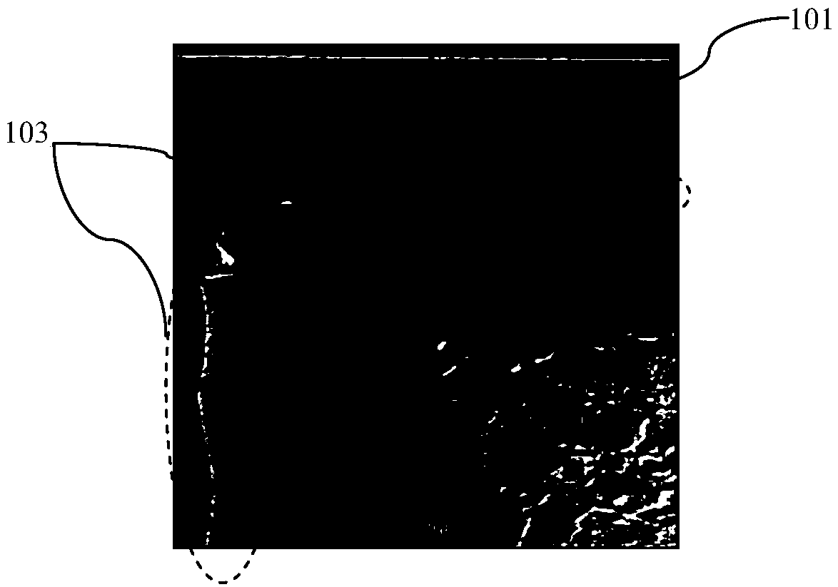
A liner and aluminum layer technology, applied in the field of semiconductor integrated circuit manufacturing, can solve problems such as difficult to remove, increase the time of dry glue removal or wet cleaning time, and the wafer cannot meet the requirements of appearance and shipment inspection.

Inactive Publication Date: 2018-03-13
SHANGHAI HUAHONG GRACE SEMICON MFG CORP
View PDF11 Cites 5 Cited by
  • Summary
  • Abstract
  • Description
  • Claims
  • Application Information

AI Technical Summary

Problems solved by technology

Simply increasing the dry degumming time or wet cleaning time is also difficult to remove
F ions in the residual polymer can combine with water vapor in the air to form HF, which increases the risk of Al corrosion
In addition, the wafer with polymer on the surface cannot meet the requirements of appearance and shipment inspection. If the polymer cannot be removed, the wafer will inevitably be discarded

Method used


Image

  • Aluminum gasket etching method
  • Aluminum gasket etching method
  • Aluminum gasket etching method

Examples


Embodiment Construction

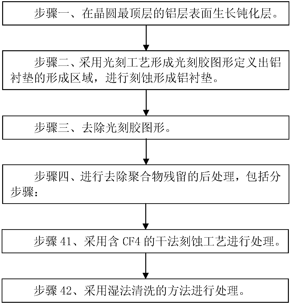
[0031] Such as figure 2 Shown is the flow chart of the method of the embodiment of the present invention; the etching method of the aluminum pad of the embodiment of the present invention includes the following steps:

[0032] Step 1, forming a topmost aluminum layer on the wafer; growing a passivation layer on the surface of the topmost aluminum layer;

[0033] In the method of the embodiment of the present invention, the wafer in step 1 is a silicon substrate wafer. Integrated circuits have been formed on the surface of the wafer.

[0034] Step 2: Forming a photoresist pattern by using a photolithography process to define an area for forming an aluminum pad, performing etching of the passivation layer and the aluminum layer to form the aluminum pad. Polymer residues are formed during the process of forming the aluminum liner; moreover, some products have more residual polymers formed during the etching process. Preferably, the thickness of the aluminum layer is more than...


PUM


Abstract

The invention discloses an aluminum gasket etching method. The aluminum gasket etching method comprises the following steps of 1, enabling a passivation layer to be grown on the surface of an aluminumlayer on the topmost layer of a wafer; 2, forming a photoresist pattern by adopting a photoetching process to define a formation region of the aluminum gasket, and performing etching to form the aluminum gasket; 3, removing the photoresist pattern; and step 4, performing post treatment of polymer residue removal, and comprising the sub steps of step 41, performing treatment by adopting a CF4-comprising dry etching process; and step 42, performing treatment by adopting a wet cleaning method. By virtue of the aluminum gasket etching method, polymer residue can be removed effectively, so that the delivery problem caused by polymer residue can be avoided, and the problem of aluminum corrosion caused by existence of the polymer after delivery can be lowered.

Description

technical field [0001] The invention relates to a method for manufacturing a semiconductor integrated circuit, in particular to an etching method for an aluminum pad. Background technique [0002] Semiconductor integrated circuits are integrated on the same wafer (wafer), which is usually a silicon substrate wafer. The integrated circuits on the wafer are drawn out through the metal layer, and a pad (PAD) is formed on the top metal layer. pad and external circuit connections. [0003] In the existing process, PAD is usually formed by photolithographic etching of metal aluminum (Al). For the PAD etching process with a transmission rate > 30% and an Al thickness > 25k angstrom, it is necessary to use a thicker Photoresist, because the photoresist is thicker, the etching time is long, and there are more polymers formed after etching. Even after dry stripping and wet stripping, it is difficult to effectively remove the polymer. If it is removed cleanly, it will affect th...

Claims


Application Information

Patent Timeline
IPC IPC(8): H01L21/02H01L21/311H01L21/60
CPCH01L21/02071H01L21/31138H01L24/11H01L2224/11614H01L2224/1181
Inventor 苏允峰
Owner SHANGHAI HUAHONG GRACE SEMICON MFG CORP
Learn More