Method for preparing grooved gate of transistor and high-power radio frequency device

A groove gate and transistor technology, which is applied in semiconductor devices, semiconductor/solid-state device manufacturing, electrical components, etc., can solve the problem of low resolution of stepper projection lithography

Active Publication Date: 2020-07-17
SUZHOU INST OF NANO TECH & NANO BIONICS CHINESE ACEDEMY OF SCI
View PDF9 Cites 0 Cited by
  • Summary
  • Abstract
  • Description
  • Claims
  • Application Information

AI Technical Summary

Problems solved by technology

The stepper projection lithography machine has high lithography efficiency and can be applied to large-area lithography, but compared with electron beam lithography, the resolution of stepper projection lithography is low

Method used


Image

  • Method for preparing grooved gate of transistor and high-power radio frequency device
  • Method for preparing grooved gate of transistor and high-power radio frequency device
  • Method for preparing grooved gate of transistor and high-power radio frequency device

Examples


Embodiment Construction

[0037] In order to enable those skilled in the art to better understand the technical solution of the present invention, a method for preparing a groove gate of a transistor and a high-power radio frequency device provided by the present invention will be further described in detail below in conjunction with the accompanying drawings and specific embodiments. In the drawings, the thicknesses of layers and regions are exaggerated for device clarity, and the same reference numerals are used to refer to the same elements throughout the specification and drawings.

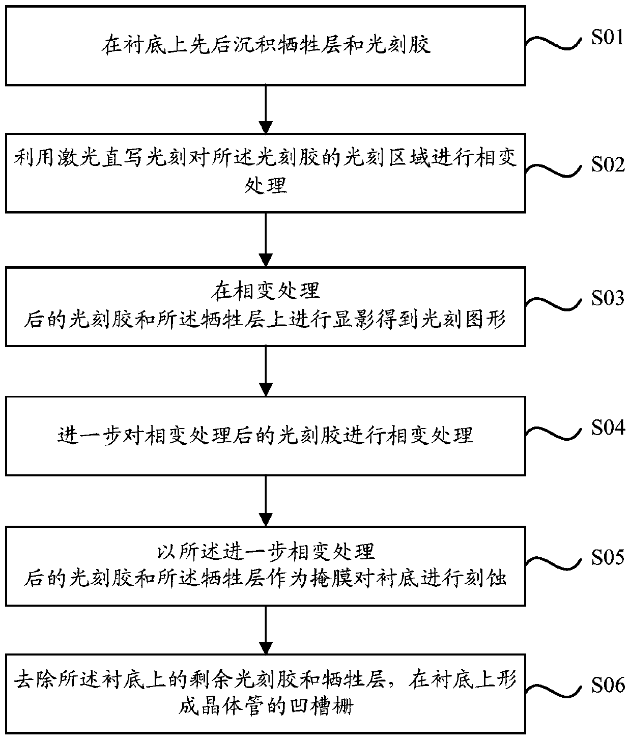
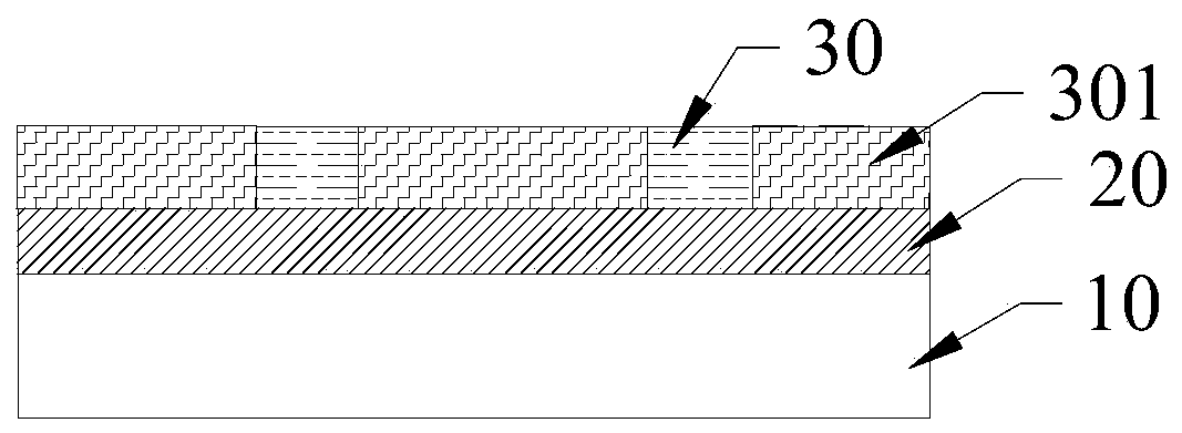
[0038] refer to figure 1 , an embodiment of the preparation method of the groove gate of the transistor of the present invention includes the following steps:

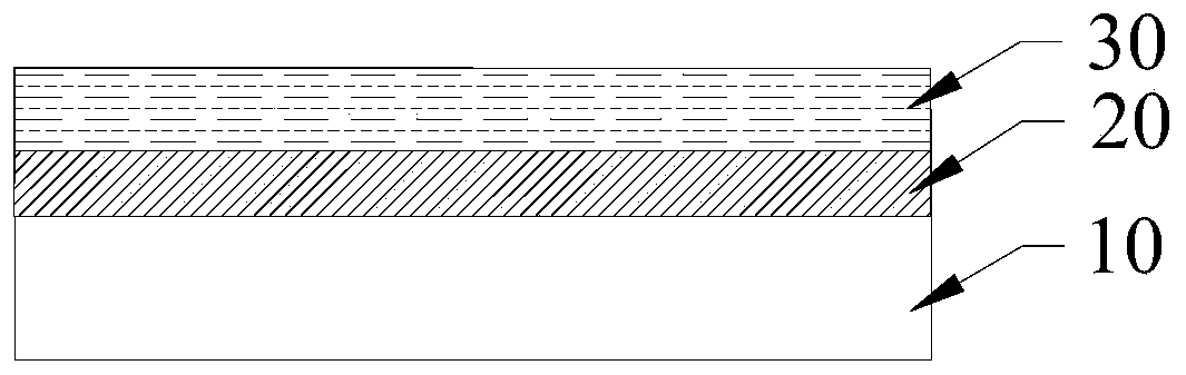
[0039] S01. Depositing a sacrificial layer and a photoresist successively on the substrate.

[0040] Using gallium nitride (GaN) as the substrate, the GaN substrate is deposited by atomic layer deposition, plasma enhanced chemical vapor deposition, electricall...


PUM

PropertyMeasurementUnit
thicknessaaaaaaaaaa
thicknessaaaaaaaaaa

Abstract

The invention discloses a method for preparing a groove gate of a transistor and a high-power radio frequency device. The preparation method comprises successively depositing a sacrificial layer and a photoresist on a substrate; using laser direct writing lithography to perform phase change treatment on the photoresist area of ​​the photoresist; after the phase change, the photoresist and the sacrificial developing on the layer to obtain a photolithographic pattern; further performing a phase change treatment on the photoresist after the phase change treatment; using the photoresist after the further phase change treatment and the sacrificial layer as a mask to etch the substrate ; Removing the remaining photoresist and the sacrificial layer on the substrate to form a grooved gate of the transistor on the substrate. Since the laser direct writing lithography technology has the advantages of narrow line width and fast writing rate, the present invention uses the laser direct writing lithography technology to prepare the groove grid, which can ensure that the obtained groove grid has narrow lithography lines and can Realize the fabrication of large area short gate length transistors.

Description

technical field [0001] The invention relates to the technical field of transistor preparation, in particular to a method for preparing a groove gate of a transistor and a high-power radio frequency device. Background technique [0002] Wide bandgap semiconductors have the characteristics of large bandgap width, high breakdown field strength, high thermal conductivity, and high electron saturation drift velocity, and have great potential in the field of high temperature and microwave power device manufacturing. Among them, GaN-based high electron mobility transistors (HEMTs) have obvious advantages in microwave high-power and high-temperature applications, and have become one of the current research hotspots. [0003] In the microwave field, the frequency characteristic of the transistor is directly related to the length of the gate electrode of the transistor; the shorter the gate length of the transistor is, the higher the frequency characteristic of the transistor is. At ...

Claims


Application Information

Patent Timeline
Patent Type & Authority Patents(China)
IPC IPC(8): H01L21/28H01L29/423H01L29/778
CPCH01L21/28H01L29/423H01L29/778
Inventor 黄荣于国浩黄源清张宝顺丁孙安
Owner SUZHOU INST OF NANO TECH & NANO BIONICS CHINESE ACEDEMY OF SCI
Why Eureka
Try Eureka