Supercharge Your Innovation With Domain-Expert AI Agents!

PCI9054-based multi-bus communication board card circuit and control method thereof

A multi-bus and circuit technology, applied in general control systems, program control, computer control, etc., can solve single problems, achieve high integration, optional bus communication methods, and reduce board design costs.

Pending Publication Date: 2018-03-16
国营芜湖机械厂
View PDF6 Cites 2 Cited by
  • Summary
  • Abstract
  • Description
  • Claims
  • Application Information

AI Technical Summary

Problems solved by technology

[0004] The technical problem to be solved by the present invention is that most of the PCI bus cards that exist on the market can only realize the communication of a single bus, and the research on multi-bus communication boards with PCI bus + 1 road RS232 bus + 3 road RS422 buses has been neglected for a long time. , the present invention is aimed at the current development status of the current PCI bus communication module, in order to grasp the design of the PCI board and its communication principle, develop a multi-bus communication card based on the PCI interface, on the basis of carrying out the system for PCI9054 and its PCI card development process , using PCI9054-bit PCI interface protocol chip, using CycloneⅢ series FPGA (EP3C5E144C8) bit local bus controller, using "FPGA+PCI9054" architecture, to design a multi-bus communication based on PCI interface with 1 RS232 and 3 RS422 transceivers Card, give the hardware design and software development of this module (including the PC test software based on VC++ and the board code based on Verilog), and test and verify its communication function

Method used


Image

  • PCI9054-based multi-bus communication board card circuit and control method thereof
  • PCI9054-based multi-bus communication board card circuit and control method thereof
  • PCI9054-based multi-bus communication board card circuit and control method thereof

Examples


Embodiment Construction

[0030] In order to make the technical means, creative features, goals and effects achieved by the present invention easy to understand, the present invention will be further elaborated below.

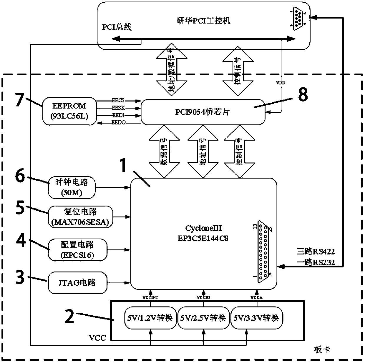
[0031] Such as figure 1 The overall schematic shown:

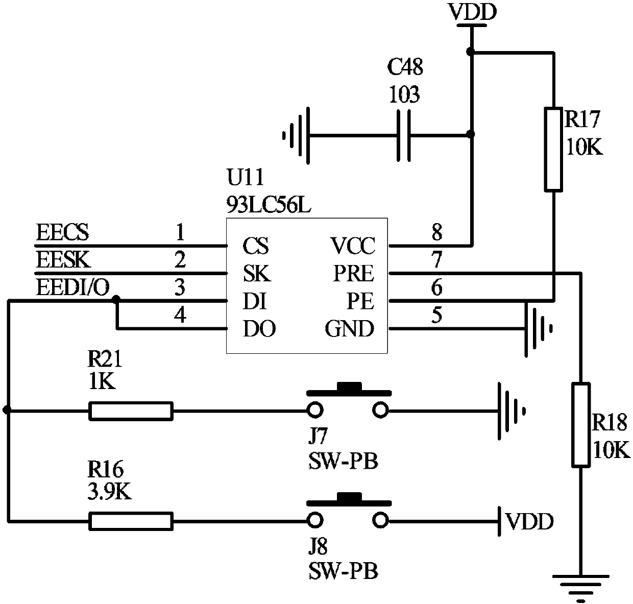
[0032] Main chip 1 adopts Cyclone III series FPGA (EP3C5E144C8 chip) chip, and the minimum system circuit design of described main chip 1 comprises clock circuit 6, reset circuit 7, JTAG circuit 3, configuration circuit 4, power supply circuit 2, and described clock circuit 6 The clock signal is generated by a 50MHz active crystal oscillator, which provides a stable clock signal for the main chip 1. The reset circuit 7 consists of a low-level reset chip MAX706SESA, and the reset circuit 7 can reset the main chip when the power is turned on. , and can also give a reset signal when the power supply is detected to be powered off or short-circuited instantaneously, and has the function of releasing the reset signal when the power suppl...


PUM


Abstract

The invention relates to a PCI9054-based multi-bus communication board card circuit and a control method thereof. The PCI9054-based multi-bus communication board card circuit comprises a master chip,a power supply circuit, a JTAG circuit, a configuration circuit, a reset circuit, a clock circuit, an EEPROM circuit, a PCI interface circuit and an interface. The master chip is connected with the power supply circuit, the JTAG circuit, the configuration circuit, the reset circuit and the clock circuit; the EEPROM circuit provides configuration information for a PCI chip; the configuration circuit provides configuration information for the master chip FPGA chip; a board card and an upper computer transmit a command frame and a data frame through DMA, and through FPGA analysis of the command frame, transmission direction is determined and RS232 and RS422 channels are selected to transmit data. The provided multi-bus board card solution based on a PCI bus +1 path of RS232 bus +3 paths of RS422 buses can realize mutual communication between the PCI bus and the RS232 bus and the RS422 buses; and the PCI9054-based multi-bus communication board card circuit has the advantages of high integration level, selectable bus communication mode and reducing board card design cost and the like, and can be widely applied to various bus test systems.

Description

technical field [0001] The invention relates to the field of multi-bus board communication, in particular to a PCI9054-based multi-bus communication board circuit and a control method. Background technique [0002] Developed from the ISA bus, the PCI bus has the characteristics of strong transmission capability, multi-bus coexistence, independence from the CPU, and automatic identification and configuration of peripherals. It is currently widely used in industrial control test systems. [0003] At present, the design of PCI has always been one of the research hotspots of many scholars. Among them, the Chinese invention patent "A High-speed Data Communication Interface Card for PCI Bus" applied by He Huinong of Hangzhou Yiheng Technology Co., Ltd. For 20051123, a PCI bus board card developed by adopting the CPLD+PCI9054 scheme is disclosed. The Chinese invention patent "Signal acquisition board suitable for multi-bus protocol and multi-expansion interface" applied by Chen Xin...

Claims


Application Information

Patent Timeline
IPC IPC(8): G05B19/042
CPCG05B19/0423G05B2219/25257
Inventor 郑永龙周勇军姚旭成彭虎张子明
Owner 国营芜湖机械厂
Features
  • R&D
  • Intellectual Property
  • Life Sciences
  • Materials
  • Tech Scout
  • Unparalleled Data Quality
  • Higher Quality Content
  • 60% Fewer Hallucinations
Learn More