Double-bracket-shaped gate-controlled bidirectional switching tunneling transistor and manufacturing method thereof

A technology of tunneling transistors and bidirectional switches, which is applied in semiconductor/solid-state device manufacturing, semiconductor devices, electrical components, etc., and can solve the problems that transistors can only be used as one-way switches and subthreshold swings cannot be reduced.

Active Publication Date: 2018-03-16
宿松新驱光电科技有限公司
View PDF3 Cites 0 Cited by
  • Summary
  • Abstract
  • Description
  • Claims
  • Application Information

AI Technical Summary

Problems solved by technology

[0004] In order to effectively combine and utilize the advantages of interchangeable source and drain of MOSFETs type devices and the low subthreshold swing swing of ordinary tunneling field effect transistors, solve the problem that the subthreshold swing of MOSFETs type devices cannot be reduced and ordinary tunneling field effect transistors Can only be used as a one-way switch, the present invention proposes a double-bracket-shaped gate-controlled bidirectional switch tunneling transistor and its manufacturing method

Method used


Image

  • Double-bracket-shaped gate-controlled bidirectional switching tunneling transistor and manufacturing method thereof
  • Double-bracket-shaped gate-controlled bidirectional switching tunneling transistor and manufacturing method thereof
  • Double-bracket-shaped gate-controlled bidirectional switching tunneling transistor and manufacturing method thereof

Examples


Embodiment Construction

[0054] Below in conjunction with accompanying drawing, the present invention will be further described:

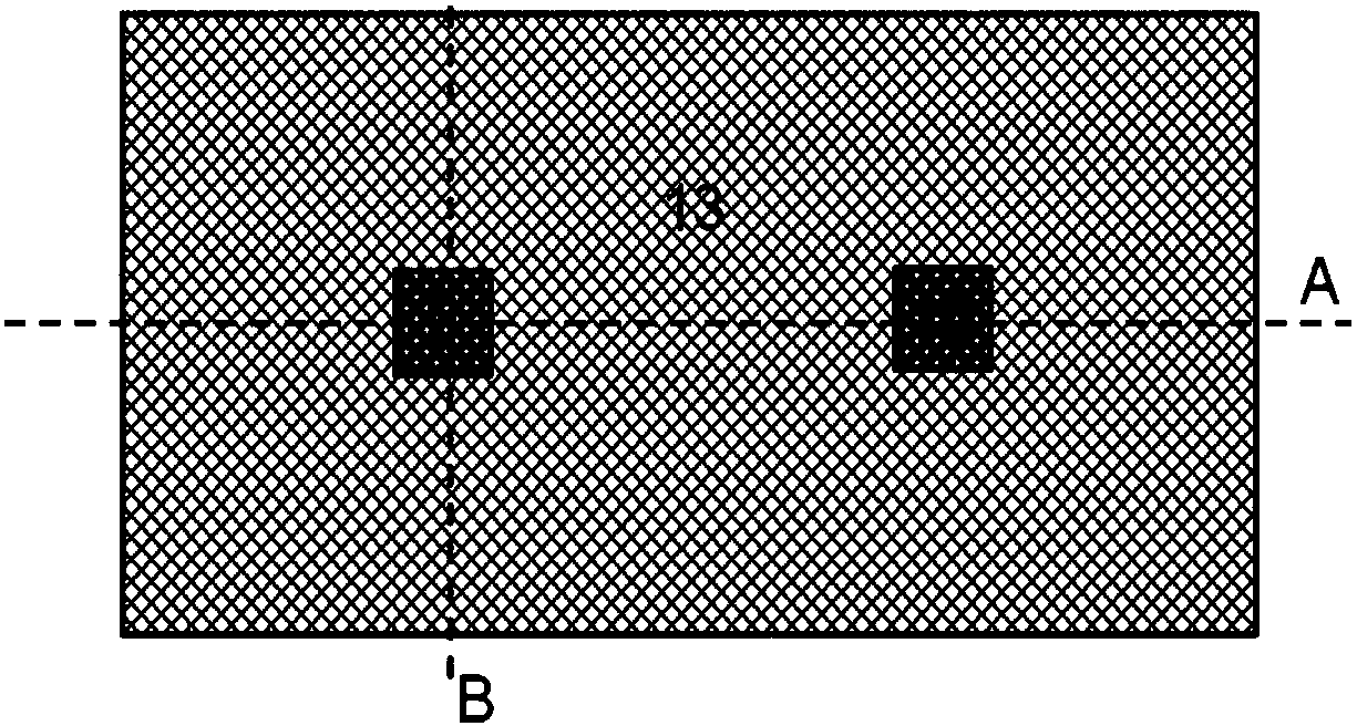
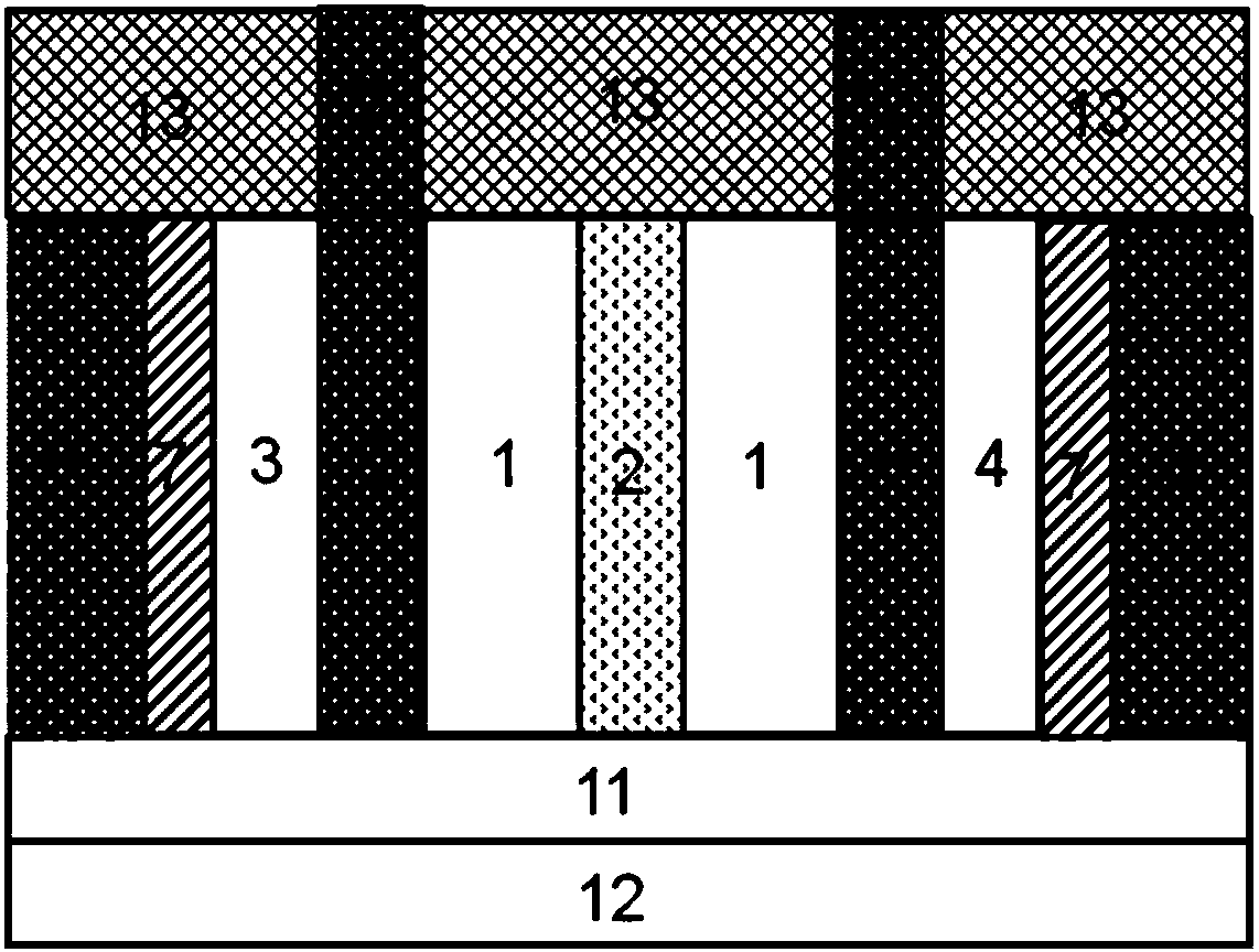
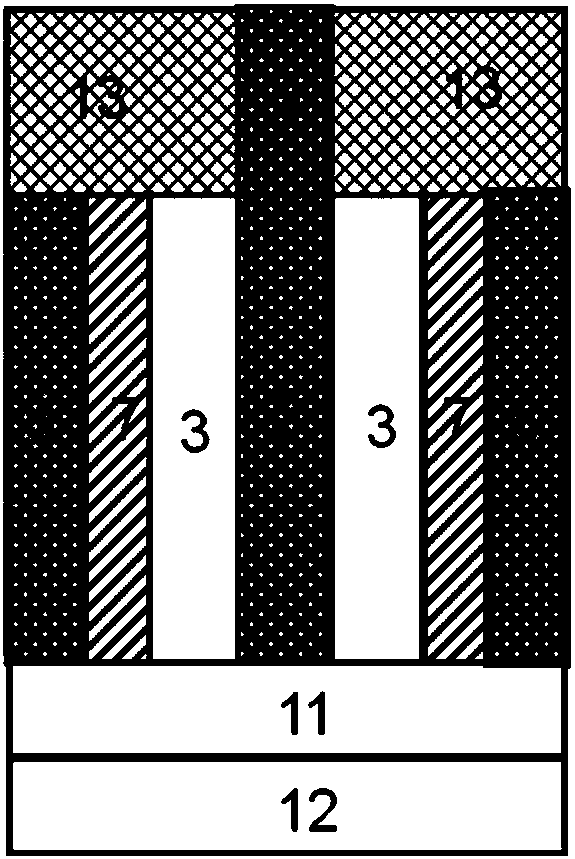
[0055] Such as figure 1 , figure 2 with image 3 As shown, a double-bracket-shaped gate-controlled bidirectional switch tunneling transistor includes a silicon substrate 12 of an SOI wafer, and the silicon substrate 12 of the SOI wafer is a substrate insulating layer 11 of the SOI wafer. Above the substrate insulating layer 11 are single crystal silicon thin film 1, heavily doped region 2 of the first type of impurity, source-drain interchangeable intrinsic region a3, source-drain interchangeable intrinsic region b4, second type impurity Partial regions of heavily doped source-drain interchangeable region a5, heavily doped source-drain interchangeable region b6 of the second type of impurity, gate electrode insulating layer 7, bracketed gate electrode 8 and insulating dielectric barrier layer 13; wherein, The heavily doped region 2 of the first type of impurity is loca...


PUM


Abstract

The invention relates to a double-bracket-shaped gate-controlled bidirectional switching tunneling transistor and a manufacturing method thereof. The transistor has a bracket gate and a left-right symmetric structural feature; the gate control capability is high; and a second type of impurity-heavily-doped source-drain exchangeable region is controlled to be as a source region or a drain region byadjusting a source-drain exchangeable electrode voltage and the tunneling current direction is changed. The transistor has advantages of low static power consumption, reverse leakage current, high gate control capability, low sub-threshold swing, and bi-directional switching. Compared with the ordinary MOSFETs type device, the transistor has the improved switching characteristic by using the tunneling effect; and compared with the common tunneling field-effect transistor, the transistor has the good bidirectional symmetric switching characteristic with the source / drain exchanging, wherein thecommon tunneling field-effect transistor does not have the characteristic. Therefore, the bidirectional switching tunneling transistor is suitable for promotion widely.

Description

technical field [0001] The invention relates to the field of ultra-large-scale integrated circuit manufacturing, in particular to a double-bracket-shaped gate-controlled bidirectional switch tunneling transistor with low leakage current suitable for low-power integrated circuit manufacturing and a manufacturing method thereof. Background technique [0002] According to the requirements of Moore's law, the basic unit MOSFETs of integrated circuits will become smaller and smaller in size, which will not only increase the difficulty of the manufacturing process, but also cause various adverse effects to become more prominent. Due to the limitations of the physical mechanism of current generation in the MOSFETs used in IC design today, the subthreshold swing cannot be lower than 60mV / dec. When the ordinary tunneling field effect transistor is used as a switching device, the tunneling effect of carriers between the semiconductor energy bands is used as the conduction mechanism of...

Claims


Application Information

Patent Timeline
Patent Type & Authority Applications(China)
IPC IPC(8): H01L29/78H01L21/336H01L29/06H01L29/417
CPCH01L29/0684H01L29/41725H01L29/66477H01L29/7833
Inventor 靳晓诗高云翔刘溪
Owner 宿松新驱光电科技有限公司
Why Eureka
Try Eureka