Double-sided folded gate-controlled source-drain double-tunneling bidirectional conduction transistor and manufacturing method thereof

A bidirectional conduction, source-drain technology, applied in semiconductor/solid-state device manufacturing, semiconductor devices, electrical components, etc., can solve the problems that transistors can only be used as one-way switches and sub-threshold swings cannot be reduced, and achieve excellent gate electrodes Control ability, effect of low subthreshold swing

Active Publication Date: 2019-10-15
深圳市永利杰科技有限公司
View PDF4 Cites 0 Cited by
  • Summary
  • Abstract
  • Description
  • Claims
  • Application Information

AI Technical Summary

Problems solved by technology

[0004] In order to effectively combine and utilize the advantages of interchangeable sources and drains of MOSFETs type devices and the low subthreshold swing of ordinary tunneling field effect transistors, solve the problem that the subthreshold swing of MOSFETs type devices cannot be reduced and ordinary tunneling field effect transistors can only As the deficiency of the unidirectional switch, the present invention proposes a double-sided folded gate-controlled source-drain double-tunneling bidirectional conduction transistor and its manufacturing method

Method used


Image

  • Double-sided folded gate-controlled source-drain double-tunneling bidirectional conduction transistor and manufacturing method thereof
  • Double-sided folded gate-controlled source-drain double-tunneling bidirectional conduction transistor and manufacturing method thereof
  • Double-sided folded gate-controlled source-drain double-tunneling bidirectional conduction transistor and manufacturing method thereof

Examples


Embodiment Construction

[0096] Below in conjunction with accompanying drawing, the present invention will be further described:

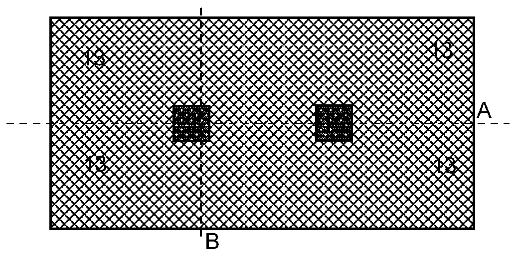
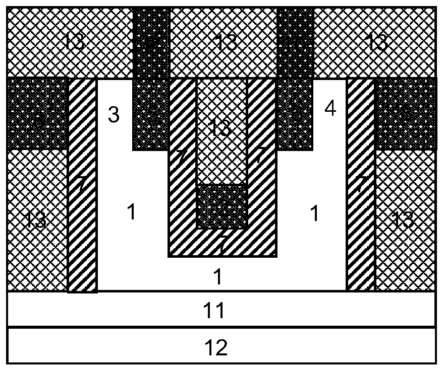
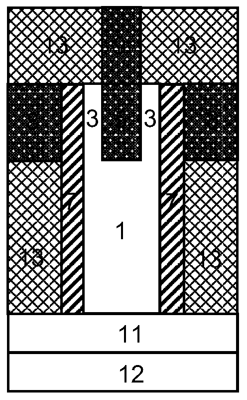
[0097] Such as figure 1 , figure 2 and image 3 As shown, a double-side folded gate-controlled source-drain double-tunneling bidirectional conduction transistor includes a silicon substrate 12 of an SOI wafer, and a substrate insulating layer 11 of the SOI wafer is above the silicon substrate 12 of the SOI wafer. , above the substrate insulating layer 11 of the SOI wafer is a single crystal silicon film 1, a barrier adjustment gate 2, a partial area of ​​the gate electrode insulating layer 7 and a partial area of ​​the insulating dielectric barrier layer 13; wherein, the single crystal silicon thin film 1 For impurity concentration below 10 16 cm -3 The monocrystalline silicon semiconductor material has a U-shaped groove structure; the heavily doped source-drain interchangeable region a5 and the heavily doped source-drain interchangeable region b6 perform ion implanta...


PUM


Abstract

The invention relates to a double-sided-folded gate-controlled source / drain double tunneling type bidirectional conductive transistor and a manufacturing method thereof. The bidirectional conductive transistor has a double-sided folded gate enabling tunneling effects to occur at the source and drain sides of the transistor simultaneously and a left-right symmetric structural feature capable of realizing source / drain exchanging and bidirectional conduction. The double-sided folded gate forms three-side coating on the vertical parts of the two sides of the monocrystalline silicon film, so that the high gate control capability and the low-sub-threshold oscillation range characteristic is realized. A barrier adjustment gate structural feature capable of preventing most of carriers in a source-drain doped region from flowing through the transistor is formed. Compared with the common MOSFETs type device, the bidirectional conductive transistor has the improved switching characteristic by using the tunneling effect; and compared with the common tunneling field-effect transistor, the bidirectional conductive transistor has the good bidirectional switching characteristic with the source / drain symmetric exchanging, wherein the common tunneling field-effect transistor does not have the characteristic. Therefore, the bidirectional conductive transistor is suitable for promotion widely.

Description

technical field [0001] The invention relates to the field of ultra-large-scale integrated circuit manufacturing, in particular to a double-sided folding gate-controlled source-drain double-tunneling bidirectional conduction transistor with low leakage current suitable for low-power integrated circuit manufacturing and a manufacturing method thereof. Background technique [0002] According to the requirements of Moore's law, the basic unit MOSFETs of integrated circuits will become smaller and smaller in size, which will not only increase the difficulty of the manufacturing process, but also cause various adverse effects to become more prominent. Due to the limitations of the physical mechanism of current generation in the MOSFETs used in IC design today, the subthreshold swing cannot be lower than 60mV / dec. When the ordinary tunneling field effect transistor is used as a switching device, the tunneling effect of carriers between the semiconductor energy bands is used as the ...

Claims


Application Information

Patent Timeline
Patent Type & Authority Patents(China)
IPC IPC(8): H01L29/78H01L29/06H01L21/336
Inventor 靳晓诗王艺澄刘溪
Owner 深圳市永利杰科技有限公司
Why Eureka
Try Eureka